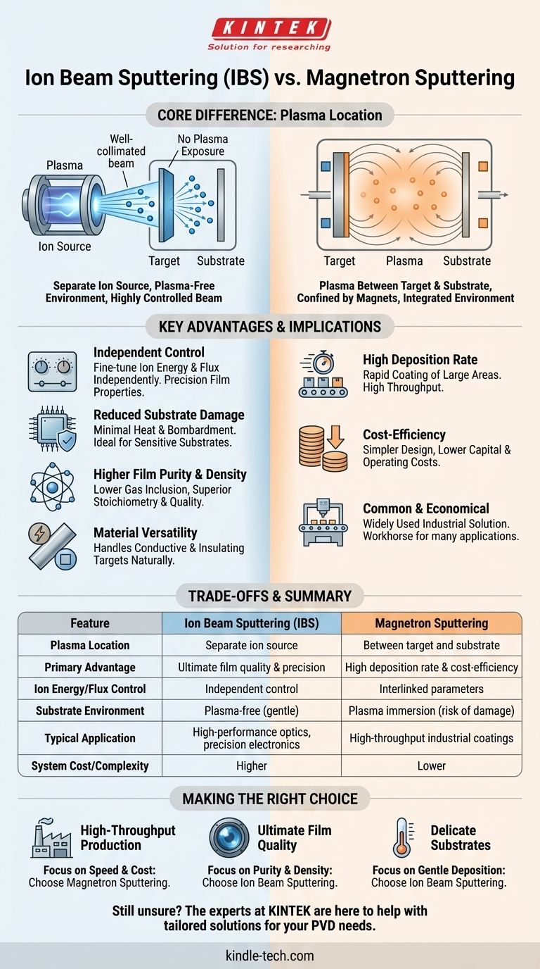
At its core, the difference between ion beam and magnetron sputtering is the location of the plasma used to generate ions. In magnetron sputtering, a plasma is created and confined by a magnetic field directly between the coating material (target) and the object being coated (substrate). In ion beam sputtering (IBS), the plasma is contained within a separate, dedicated ion source that generates a focused beam of ions, which is then directed at the target in a plasma-free environment.
The fundamental distinction is one of control. By separating the ion generation from the target and substrate, ion beam sputtering decouples key process parameters, offering a level of precision and film quality that is difficult to achieve with the integrated plasma environment of magnetron sputtering.
The Core Architectural Difference
The primary divergence between these two physical vapor deposition (PVD) techniques stems from how and where they generate the energetic ions that dislodge material from a target.
How Magnetron Sputtering Works: A Confined Plasma
In magnetron sputtering, the chamber is filled with an inert gas, typically Argon. A strong negative voltage is applied to the target material.
This high voltage ignites the gas into a plasma—a cloud of positive ions and free electrons. A magnetic field behind the target traps the electrons, dramatically increasing the plasma density near the target surface.
These positive ions are then accelerated into the negatively charged target, striking it with enough force to knock off, or "sputter," atoms. These sputtered atoms travel through the plasma-filled space and deposit onto the substrate, forming a thin film.
How Ion Beam Sputtering Works: A Dedicated Ion Source
Ion beam sputtering (IBS) physically separates the process into two distinct zones. The ion source contains the plasma and is responsible for generating and accelerating a uniform, well-collimated beam of ions.
This ion beam is then directed out of the source and across a vacuum space toward the target. The target and substrate are not immersed in plasma.
When the ion beam strikes the target, it sputters material in a highly controlled manner. Because the ions arrive with a specific energy and angle, the sputtering process is exceptionally predictable and uniform.
Key Implications for Film Quality and Process Control
This architectural difference has profound consequences for the deposition process and the resulting quality of the thin film.
Independent Control (IBS Advantage)
In ion beam sputtering, you can independently control the ion energy (how hard the ions hit) and the ion flux (how many ions hit the target per second). This allows for fine-tuning the deposition process to achieve specific film properties.
In magnetron sputtering, these parameters are interlinked with the plasma's operating pressure and power, making independent optimization much more challenging.
Reduced Substrate Damage (IBS Advantage)
Because the substrate is not exposed to a plasma in an IBS system, there is significantly less risk of damage from heat or bombardment by stray high-energy particles. This makes IBS ideal for depositing films onto sensitive substrates, such as delicate optics or temperature-sensitive electronics.
Higher Film Purity and Density (IBS Advantage)
The plasma in magnetron sputtering can lead to some of the inert gas atoms becoming embedded in the growing film, which can compromise its purity and properties.
IBS operates in a higher vacuum environment with no plasma near the substrate, resulting in significantly lower gas inclusion. The controlled energy of the arriving ions also helps create denser, more stable, and higher-quality films with superior stoichiometry.
Material Versatility
Both techniques are versatile. However, for sputtering insulating (non-conductive) materials, magnetron sputtering typically requires an RF (Radio Frequency) power supply to prevent charge buildup on the target.
IBS naturally handles both conducting and insulating materials without modification because the target is not part of an electrical circuit and is simply a material to be struck by the ion beam.
Understanding the Trade-offs
Choosing a sputtering technique requires balancing ideal film properties with practical production requirements.
Deposition Rate vs. Precision
Magnetron sputtering generally offers a much higher deposition rate, making it more suitable for rapidly coating large areas. It is the workhorse for many industrial applications where throughput is critical.
Ion beam sputtering is a slower, more deliberate process. Its value lies in unmatched precision and film quality, not speed.
System Complexity and Cost
Magnetron sputtering systems are simpler in design, more common, and significantly more economical to purchase and operate.
IBS systems are more complex due to the dedicated ion source and associated high-vacuum requirements. This translates to a higher capital investment and maintenance overhead.
Making the Right Choice for Your Goal
Your decision ultimately depends on the non-negotiable requirements of your specific application.
- If your primary focus is high-throughput production or cost-efficiency: Magnetron sputtering is almost always the superior choice for coating large areas quickly and economically.
- If your primary focus is ultimate film quality, purity, and density: Ion beam sputtering is the definitive choice for demanding applications like high-performance optical coatings, precision electronics, and research.
- If your primary focus is depositing on delicate or temperature-sensitive substrates: Ion beam sputtering provides a gentler, more controlled environment that minimizes the risk of damage.
Your choice hinges on balancing the need for ultimate film performance against the practical constraints of deposition speed and cost.
Summary Table:
| Feature | Ion Beam Sputtering (IBS) | Magnetron Sputtering |
|---|---|---|
| Plasma Location | Separate ion source | Between target and substrate |
| Primary Advantage | Ultimate film quality & precision | High deposition rate & cost-efficiency |
| Ion Energy/Flux Control | Independent control | Interlinked parameters |
| Substrate Environment | Plasma-free (gentle on substrates) | Plasma immersion (risk of damage) |
| Typical Application | High-performance optics, sensitive electronics | High-throughput industrial coatings |
| System Cost/Complexity | Higher | Lower |
Still unsure which sputtering technique is right for your specific application? The experts at KINTEK are here to help. We specialize in providing lab equipment and consumables, offering tailored solutions for your unique laboratory needs. Whether you require the ultimate precision of ion beam sputtering or the high-throughput capabilities of magnetron sputtering, we can guide you to the optimal PVD solution. Contact our technical team today to discuss your project requirements and discover how KINTEK can enhance your thin film deposition process.
Visual Guide