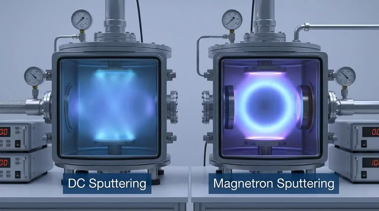
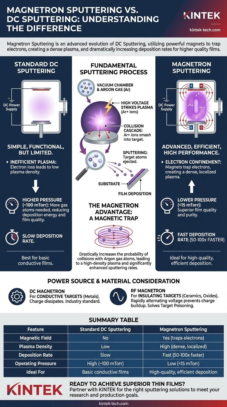
At its core, the difference between magnetron sputtering and standard DC sputtering is the addition of a powerful magnetic field. Magnetron sputtering is an advanced form of DC sputtering that uses magnets placed behind the target material. This magnetic field traps electrons close to the target, creating a much denser plasma that dramatically increases the rate at which atoms are "sputtered" onto your substrate.
While basic DC sputtering provides a simple mechanism for depositing conductive films, it is relatively slow and inefficient. Magnetron sputtering is the modern evolution, using a magnetic field to supercharge the process, enabling faster deposition rates at lower pressures and ultimately yielding higher quality films.
The Fundamental Sputtering Process
To understand the magnetron advantage, we must first look at the core principles of sputtering. This physical vapor deposition (PVD) process is a "billiard ball" game on an atomic scale.
How Sputtering Begins: The Role of Plasma
First, a vacuum chamber is filled with a small amount of an inert gas, typically Argon (Ar). A high negative DC voltage is applied to the target material you wish to deposit. This voltage strikes a plasma, stripping electrons from the Argon atoms and leaving behind positively charged Argon ions (Ar+).
The Collision Cascade
These positive Ar+ ions are then accelerated by the strong electric field and smash into the negatively charged target. This high-energy impact transfers kinetic energy to the target atoms. If enough energy is transferred, target atoms are physically knocked loose from the surface, a process called sputtering. These ejected atoms then travel through the vacuum chamber and deposit as a thin film on your substrate.
Why "Standard" DC Sputtering Has Limitations
A simple DC sputtering system (often called diode sputtering) without magnets is functional but faces significant performance hurdles that limit its modern applications.
Inefficient Plasma
Without a magnetic field, many of the free electrons in the plasma travel directly to the substrate or chamber walls. This electron loss means fewer collisions with Argon atoms, resulting in a less dense, less efficient plasma.
Higher Pressure Requirement
To compensate for this inefficiency, standard DC systems must operate at higher gas pressures (e.g., ~100 mTorr). More gas atoms in the chamber increase the probability of collisions to sustain the plasma. However, this also means sputtered atoms are more likely to collide with gas atoms on their way to the substrate, reducing deposition energy and film quality.
The Magnetron Advantage: A Magnetic Trap
The introduction of magnets fundamentally changes the dynamics of the plasma, overcoming the core limitations of simple DC sputtering.
Confining the Electrons
The magnets create a magnetic field parallel to the target surface. This field traps the highly mobile electrons, forcing them into a spiral path near the target. This confinement drastically increases the path length of each electron within the plasma region.
Creating a Dense, Localized Plasma
Because the electrons are trapped, they have a vastly increased probability of colliding with and ionizing Argon gas atoms. This creates a dense, self-sustaining plasma concentrated in a "racetrack" pattern on the target's surface, precisely where it is most effective.
The Impact on Performance
This high-density plasma bombards the target with far more ions per second, leading to a sputtering rate that can be 50-100 times higher than a non-magnetron DC system. Furthermore, because the plasma is so efficiently sustained, the system can be operated at much lower pressures (under 15 mTorr), improving the quality and purity of the deposited film.
A Critical Distinction: Conductive vs. Insulating Materials
It is vital to distinguish the role of the power source (DC vs. RF) from the role of the magnets (magnetron). The choice of power source is determined by your target material's electrical properties.
DC Magnetron for Conductive Targets
DC sputtering, including DC magnetron, works by applying a constant negative voltage to the target. This only works if the target material is electrically conductive (like most metals), allowing the charge to dissipate.
RF Sputtering for Insulating Targets
If you try to use DC power on an insulating (dielectric) target like a ceramic or oxide, positive charge from the Argon ions builds up on the surface. This buildup, known as target poisoning, quickly neutralizes the negative voltage and stops the sputtering process entirely.
To solve this, Radio Frequency (RF) sputtering is used. It uses a high-frequency AC power source that rapidly alternates the voltage. This alternating field prevents charge from building up, allowing for the continuous sputtering of insulating materials. RF sputtering systems are very often configured as RF Magnetron systems to gain the same efficiency benefits from the magnetic field.
How to Apply This to Your Goal
Your choice of sputtering method depends entirely on the material you need to deposit and your performance requirements.
- If your primary focus is depositing conductive materials (metals) quickly and efficiently: DC magnetron sputtering is the industry standard and almost always the correct choice.
- If your primary focus is depositing insulating or dielectric materials (ceramics, oxides): You must use an RF power source. An RF magnetron system will provide the best performance and deposition rates.
- If your primary focus is a simple, low-cost setup for basic metal deposition: A standard DC diode (non-magnetron) system can work, but you will sacrifice deposition speed and film quality.
Ultimately, understanding the interplay between the power source and the magnetic plasma confinement allows you to select the precise tool needed to achieve high-quality thin films for your specific application.
Summary Table:
| Feature | Standard DC Sputtering | Magnetron Sputtering |
|---|---|---|
| Magnetic Field | No | Yes (traps electrons) |
| Plasma Density | Low | High (dense, localized) |
| Deposition Rate | Slow | Fast (50-100x faster) |
| Operating Pressure | High (~100 mTorr) | Low (<15 mTorr) |
| Ideal For | Basic conductive films | High-quality, efficient deposition |
Ready to Achieve Superior Thin Films for Your Lab?
Understanding the difference between magnetron and DC sputtering is the first step to optimizing your deposition process. KINTEK, your trusted partner in laboratory equipment, specializes in providing the right sputtering solutions to meet your specific research and production goals.
Whether you are depositing conductive metals or insulating ceramics, our expertise ensures you get the performance and quality your work demands. Let us help you select the perfect system to enhance your lab's capabilities and accelerate your results.
Contact KINTEL today to discuss your application and discover how our advanced sputtering equipment can benefit your laboratory.
Visual Guide
Related Products
- Spark Plasma Sintering Furnace SPS Furnace
- RF PECVD System Radio Frequency Plasma-Enhanced Chemical Vapor Deposition RF PECVD
People Also Ask
- What are the advantages of CAMI/SPS for W-Cu composite preparation? Reduce cycles from hours to seconds.
- What is the theory of spark plasma sintering? A Guide to Rapid, Low-Temperature Densification
- What are the fundamentals of spark plasma sintering process? Unlock Rapid, High-Performance Material Consolidation
- What is the mechanism of SPS process? A Deep Dive into Rapid, Low-Temperature Sintering
- Why are Spark Plasma Sintering (SPS) furnaces or hot presses utilized in the preparation of Li3PS4 solid electrolytes?

