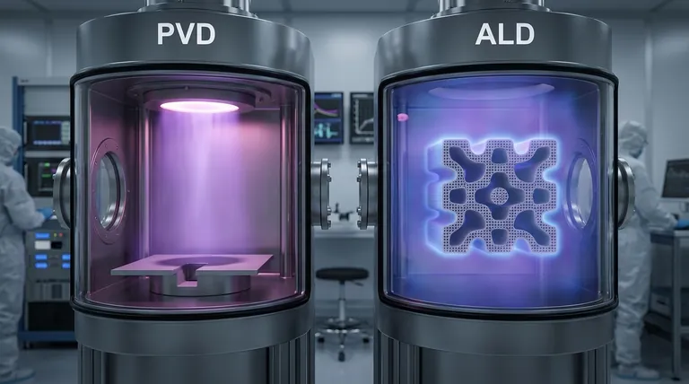
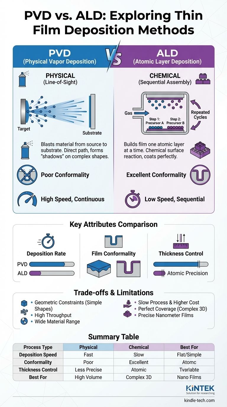
At its core, the difference between PVD and ALD comes down to how the thin film is built. Physical Vapor Deposition (PVD) is a line-of-sight physical process, like spray painting, where material is blasted from a source onto a substrate. Atomic Layer Deposition (ALD), conversely, is a chemical process that builds the film one single atomic layer at a time, ensuring every surface is coated perfectly.
The decision between PVD and ALD is not a matter of which is superior, but which is appropriate for the task. PVD offers speed and efficiency for simpler geometries, while ALD provides unparalleled precision and complete coverage for complex, three-dimensional structures.
The Fundamental Difference: Physical vs. Chemical Processes
To choose the right method, you must first understand their fundamentally different mechanisms. One physically transfers material, while the other chemically constructs it.
How PVD Works: A Physical "Line-of-Sight" Transfer
PVD encompasses a family of techniques, like sputtering, where a source material (a "target") is bombarded with high-energy particles.
This bombardment physically knocks atoms or molecules off the target. These ejected particles then travel in a straight line through a vacuum and condense onto the substrate, forming a thin film.
Because it relies on this direct path, PVD is a line-of-sight process. Any part of the substrate not directly visible to the source will not be coated, creating "shadows."
How ALD Works: A Sequential Chemical Assembly
ALD is a subtype of chemical vapor deposition (CVD) but with far greater control. It uses a sequence of self-limiting chemical reactions to deposit a film one atomic layer per cycle.
First, a precursor gas is introduced into the chamber and reacts with the available sites on the substrate surface. Once all sites are occupied, the reaction stops.
The chamber is then purged of excess precursor. A second precursor is introduced, which reacts with the first layer to complete a single, uniform monolayer of the desired material. This cycle is repeated to build the film to the desired thickness.
Because this process relies on gas diffusion and surface reactions, it is isotropic, meaning it coats every nook, cranny, and complex surface with perfect uniformity.
Comparing Key Attributes: Speed vs. Precision
The operational differences between PVD and ALD lead to distinct advantages in speed, coverage, and control.
Deposition Rate: The Speed of PVD
PVD is a continuous process that can deposit material very quickly. This high deposition rate makes it ideal for manufacturing thicker films or for applications where high throughput is a primary economic driver.
Film Conformality: The Perfection of ALD
Conformality is the ability of a film to maintain a uniform thickness over complex surface topography. ALD excels here, providing 100% conformal coverage on high-aspect-ratio structures like trenches and pores.
PVD, due to its line-of-sight nature, has poor conformality on such complex surfaces.
Thickness Control: The Atomic Accuracy of ALD
Since ALD builds the film one atomic layer at a time, the final thickness is simply a function of the number of cycles performed. This gives you exact, digital control over film thickness, which is critical for ultra-thin films in the nanometer range (e.g., 10-50 nm). PVD offers much less precision.
Understanding the Trade-offs and Limitations
Neither technology is a silver bullet. Your choice involves balancing their inherent strengths and weaknesses against your project's specific requirements.
PVD's Geometric Constraints
The primary limitation of PVD is its inability to coat complex, non-planar surfaces uniformly. It is best suited for flat or gently curved substrates. Attempting to coat intricate 3D objects will result in an uneven film with uncoated "shadowed" regions.
ALD's Slow Process and Higher Cost
The precision of ALD comes at the cost of speed. The sequential, multi-step cycles make it a much slower deposition method than PVD. This can be a significant drawback for applications requiring thick films or high-volume production, potentially increasing cost and process time.
Material and Process Complexity
PVD can deposit a wide range of materials, including complex alloys, with relative ease. ALD relies on the availability of suitable chemical precursors that can perform the self-limiting reactions, which can limit the palette of available materials and add process complexity.
Making the Right Choice for Your Goal
To make a definitive decision, you must map the strengths of each technology to your primary objective.
- If your primary focus is speed and coating simple surfaces: PVD is the clear choice for its high deposition rate and cost-effectiveness on flat substrates used in optics or basic electronics.
- If your primary focus is perfect uniformity on complex 3D structures: ALD is the only viable option for creating conformal, pinhole-free films inside deep trenches or on porous materials, essential for advanced semiconductors and MEMS.
- If your primary focus is ultra-precise thickness for nanometer-scale films: ALD provides the atomic-level control necessary for next-generation transistors, memory devices, and catalysts.
- If your primary focus is depositing a wide variety of metals and alloys quickly: PVD is often the more straightforward and faster method for creating custom alloy films for mechanical or electrical applications.
Ultimately, your choice is dictated by the trade-off between the geometry you need to coat and the precision you need to achieve.
Summary Table:
| Attribute | PVD (Physical Vapor Deposition) | ALD (Atomic Layer Deposition) |
|---|---|---|
| Process Type | Physical (line-of-sight) | Chemical (surface reactions) |
| Deposition Speed | Fast (continuous process) | Slow (sequential cycles) |
| Conformality | Poor (shadows on complex shapes) | Excellent (100% uniform coverage) |
| Thickness Control | Less precise | Atomic-level precision |
| Best For | Flat/simple surfaces, high throughput | Complex 3D structures, nanometer films |
Still unsure whether PVD or ALD is right for your laboratory application?
KINTEK specializes in lab equipment and consumables, serving laboratory needs with precision deposition solutions. Our experts can help you select the perfect system for your specific substrates and research goals.
Contact our team today for a personalized consultation and discover how our deposition equipment can enhance your research outcomes and operational efficiency.
Visual Guide
Related Products
- RF PECVD System Radio Frequency Plasma-Enhanced Chemical Vapor Deposition RF PECVD
- Evaporation Boat for Organic Matter
- Chemical Vapor Deposition CVD Equipment System Chamber Slide PECVD Tube Furnace with Liquid Gasifier PECVD Machine
- Electron Beam Evaporation Coating Oxygen-Free Copper Crucible and Evaporation Boat
- VHP Sterilization Equipment Hydrogen Peroxide H2O2 Space Sterilizer
People Also Ask
- Why is PECVD environment friendly? Understanding the Eco-Friendly Benefits of Plasma-Enhanced Coating
- What is the principle of plasma enhanced chemical vapor deposition? Achieve Low-Temperature Thin Film Deposition
- What is plasma activated chemical vapour deposition method? A Low-Temperature Solution for Advanced Coatings
- What is an example of PECVD? RF-PECVD for High-Quality Thin Film Deposition
- What are the benefits of PECVD? Achieve Superior Low-Temperature Thin Film Deposition