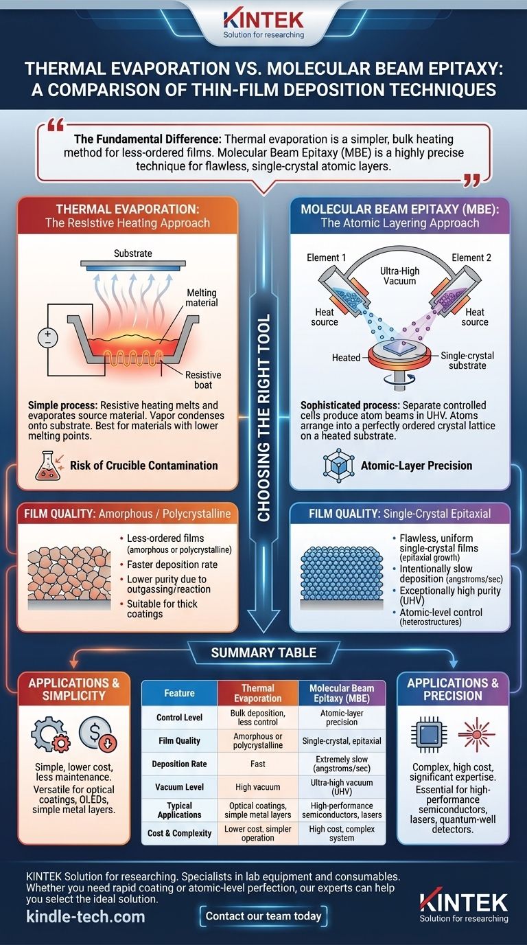
The fundamental difference between thermal evaporation and molecular beam epitaxy (MBE) is the level of control over the deposition process and the resulting quality of the thin film. Thermal evaporation is a simpler, bulk heating method that produces less-ordered films, while MBE is a highly precise technique for growing perfect, single-crystal atomic layers.
While both are methods of physical vapor deposition (PVD), the choice between them comes down to a critical trade-off: thermal evaporation offers speed and simplicity for basic coatings, whereas MBE provides atomic-level precision for creating flawless, high-performance crystalline structures.
The Core Mechanisms: Heat vs. Precision Growth
The "what" of the difference lies in how each method generates a vapor from the source material and deposits it onto a substrate. Their approaches are fundamentally different in purpose and execution.
Thermal Evaporation: The Resistive Heating Approach
Thermal evaporation is a straightforward process. An electric current is passed through a resistive boat or crucible containing the source material.
This current heats the crucible, which in turn heats the material until it melts and evaporates. The resulting vapor travels in a straight line through a vacuum and condenses on a cooler substrate, forming a thin film.
This method is best suited for materials with lower melting points. Because the entire crucible is heated, there is a higher risk of impurities from the crucible itself contaminating the final film.
Molecular Beam Epitaxy: The Atomic Layering Approach
Molecular Beam Epitaxy (MBE) is a significantly more sophisticated process conducted in an ultra-high vacuum (UHV) environment.
Instead of a single heated crucible, MBE uses separate, highly controlled heated cells for each individual element (e.g., one for gallium, one for arsenic). These cells produce beams of atoms or molecules that are aimed precisely at a heated, single-crystal substrate.
The term epitaxy means the deposited atoms arrange themselves in a perfectly ordered crystal lattice that mirrors the structure of the underlying substrate. This slow, controlled growth allows for the creation of materials one atomic layer at a time.
How Process Dictates Film Quality
The deep need behind this question is understanding why these different mechanisms matter. The choice of technique directly impacts the final film's purity, structure, and performance.
Purity and Contamination
In thermal evaporation, heating the entire crucible can cause it to outgas or react with the source material, introducing contaminants into the film.
MBE operates in an ultra-high vacuum, which is many orders of magnitude cleaner than the vacuum used for thermal evaporation. This, combined with using highly pure elemental sources, results in films with exceptionally high purity, which is critical for high-performance electronics.
Crystallinity and Structure
Thermal evaporation is a less controlled condensation process. It typically produces films that are amorphous (disordered) or polycrystalline (composed of many small, randomly oriented crystal grains).
The entire purpose of MBE is to create single-crystal films. The slow deposition rate and heated substrate give atoms the time and energy they need to find their precise place in the crystal lattice, resulting in a flawless, uniform structure.
Deposition Rate and Control
Thermal evaporation is a relatively fast deposition method, useful for applying thicker coatings quickly. However, this speed comes at the cost of fine control over thickness and composition.
MBE is an intentionally slow process, often measured in angstroms per second or monolayers per minute. This deliberation provides operators with atomic-level control over film thickness and the ability to create complex, layered structures (heterostructures) with abrupt, perfectly defined interfaces.
Understanding the Trade-offs: Simplicity vs. Perfection
Choosing between these techniques is a practical decision based on your goals, budget, and material requirements. Neither is universally "better"; they are tools for different jobs.
Cost and Complexity
Thermal evaporation systems are relatively simple, inexpensive to build and operate, and require less maintenance. They are a workhorse technology for many standard coating applications.
MBE systems are at the opposite end of the spectrum. They are extremely complex, require costly ultra-high vacuum equipment, and demand significant expertise to operate and maintain.
Application and Versatility
The simplicity of thermal evaporation makes it versatile for a wide range of applications, such as creating conductive metal layers for OLEDs or optical coatings on glass. The quality of the film is sufficient for these purposes.
MBE is a specialized tool used when crystalline perfection is non-negotiable. It is essential for fabricating high-performance semiconductor devices like high-frequency transistors, lasers, and quantum-well detectors, where even minor crystal defects would ruin device performance.
Making the Right Choice for Your Goal
Your application's requirements for film quality and structure will dictate the correct choice.
- If your primary focus is rapidly applying a simple metallic or organic coating where crystalline structure is not critical: Thermal evaporation is the more efficient and cost-effective solution.
- If your primary focus is creating a flawless, single-crystal semiconductor film for a high-performance electronic or photonic device: Molecular Beam Epitaxy is the only technique that provides the necessary atomic-level precision and purity.
Ultimately, understanding the fundamental differences in mechanism and outcome empowers you to select the right tool for achieving your specific material science or engineering goal.
Summary Table:
| Feature | Thermal Evaporation | Molecular Beam Epitaxy (MBE) |
|---|---|---|
| Control Level | Bulk deposition, less control | Atomic-layer precision |
| Film Quality | Amorphous or polycrystalline | Single-crystal, epitaxial |
| Deposition Rate | Fast | Extremely slow (angstroms/sec) |
| Vacuum Level | High vacuum | Ultra-high vacuum (UHV) |
| Typical Applications | Optical coatings, simple metal layers | High-performance semiconductors, lasers |
| Cost & Complexity | Lower cost, simpler operation | High cost, complex system |
Struggling to choose the right deposition technique for your research or production needs? KINTEK specializes in lab equipment and consumables, serving laboratories with precise thin-film deposition requirements. Whether you need the rapid coating capabilities of thermal evaporation or the atomic-level perfection of MBE systems, our experts can help you select the ideal solution to enhance your material performance and research outcomes. Contact our team today for a personalized consultation!
Visual Guide
Related Products
- Molybdenum Tungsten Tantalum Evaporation Boat for High Temperature Applications
- Aluminized Ceramic Evaporation Boat for Thin Film Deposition
- Evaporation Boat for Organic Matter
- Chemical Vapor Deposition CVD Equipment System Chamber Slide PECVD Tube Furnace with Liquid Gasifier PECVD Machine
- Customer Made Versatile CVD Tube Furnace Chemical Vapor Deposition Chamber System Equipment
People Also Ask
- What are thermal evaporation sources? Key Types and How to Choose the Right One
- How source material is evaporated during deposition? A Guide to Resistive vs. E-Beam Methods
- Is thermal evaporation used to deposit a thin metal film? A Guide to This Foundational PVD Technique
- How does a molybdenum evaporation source function in H2S for MoS2 synthesis? Master Reactive Film Deposition
- What is the source of evaporation for thin film? Choosing Between Thermal and E-Beam Methods