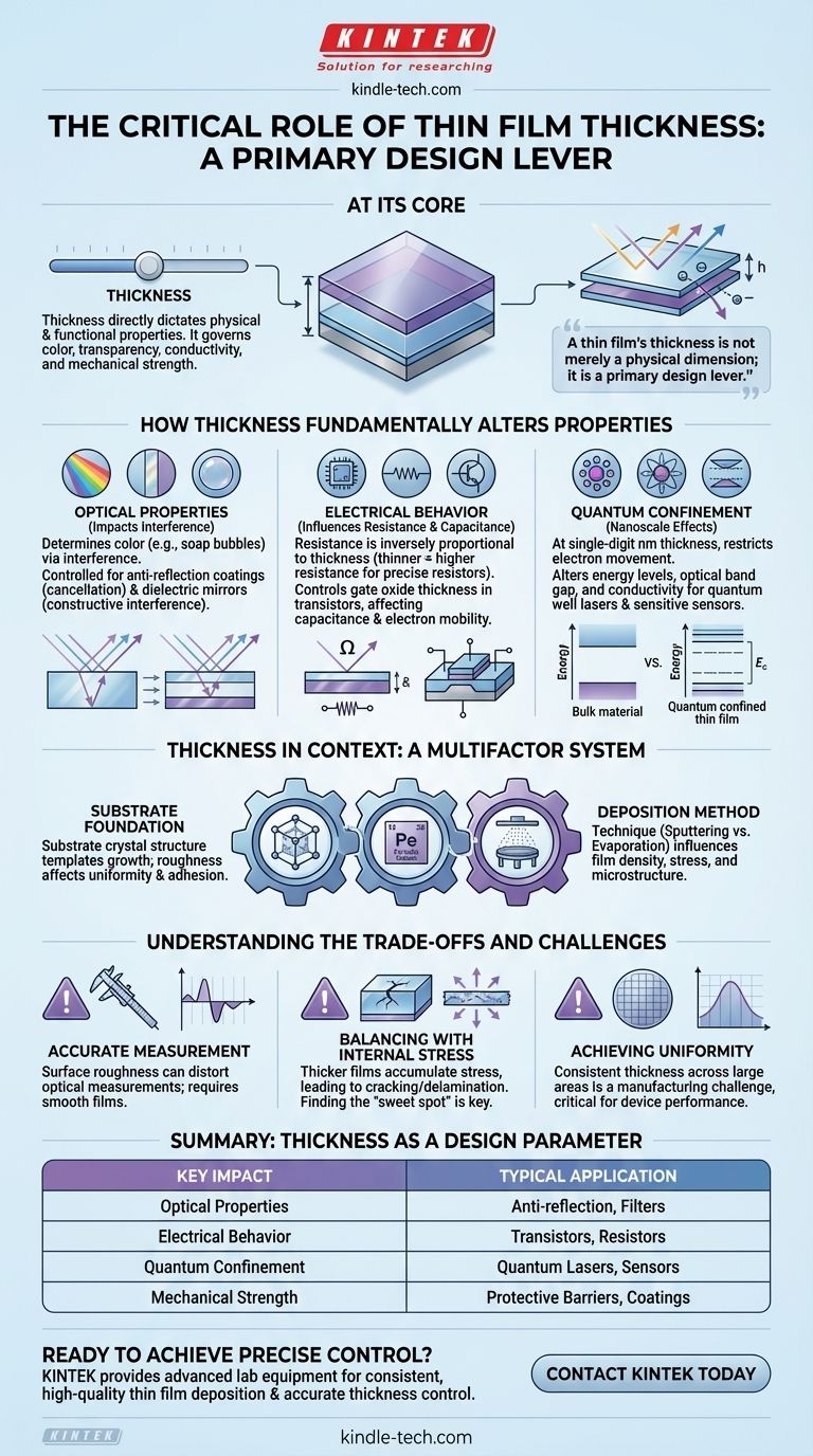
At its core, a thin film's thickness is one of the most critical parameters you can control, directly dictating its physical and functional properties. For instance, in optical applications, a film's behavior changes dramatically as its thickness varies, especially for films thinner than 80 nanometers, where interference effects become dominant. This single dimension governs everything from its color and transparency to its electrical conductivity and mechanical strength.
A thin film's thickness is not merely a physical dimension; it is a primary design lever. Changing the thickness fundamentally alters how the film interacts with light, electricity, and mechanical stress, but its effects are always in context with the film's material, its substrate, and the method used to deposit it.
How Thickness Fundamentally Alters Film Properties
The thickness of a film determines which physical phenomena become dominant. As you move from micrometers down to nanometers, you are not just making the film thinner; you are changing the rules that govern its behavior.
Impact on Optical Properties
This is the most intuitive effect of thickness. The color of a soap bubble or an oil slick on water is a direct result of thin-film interference, which is entirely dependent on the film's thickness.
For engineered coatings, this effect is precisely controlled. By tuning the thickness, you can create anti-reflection coatings, where reflected light waves cancel each other out, or dielectric mirrors, where they constructively interfere to create high reflectivity.
Influence on Electrical Behavior
In electronics, thickness is paramount. The resistance of a conductive film is inversely proportional to its thickness. Thinner films have higher resistance, a principle used to create precise resistors.
Furthermore, in semiconductor devices, the thickness of gate oxides, channel layers, and insulating layers directly controls capacitance, electron mobility, and leakage current, defining the performance of a transistor.
The Role of Quantum Confinement
When a film becomes exceptionally thin (typically in the single-digit nanometer range), its thickness approaches the wavelength of electrons.
This quantum confinement restricts electron movement in one dimension, which fundamentally changes the material's energy levels. This can alter its optical band gap and electrical conductivity in ways not seen in the bulk material, enabling technologies like quantum well lasers and highly sensitive sensors.
Thickness in Context: A Multifactor System
While thickness is a primary control knob, its effect cannot be isolated from other critical factors. The final properties of a thin film are the result of an interdependent system.
The Substrate Foundation
The film's properties are heavily influenced by the substrate it is grown on. A substrate's crystal structure can template the film's growth, and its surface roughness can affect the film's uniformity and adhesion.
The Choice of Material
The intrinsic properties of the chosen material—the target in sputtering or the source in evaporation—set the baseline. Thickness then modifies these properties.
Depositing a 50 nm film of gold will yield vastly different electrical and optical results than a 50 nm film of silicon dioxide. The material dictates the potential, and the thickness refines the outcome.
The Deposition Method
How you build the film matters. A technique like sputtering creates a dense, adherent film, while thermal evaporation may result in a more porous structure.
These microstructural differences, determined by the deposition process, will interact with the film's thickness to influence its final density, internal stress, and environmental stability.
Understanding the Trade-offs and Challenges
Controlling thickness is not without its difficulties. Achieving the desired dimension consistently and reliably requires navigating several practical challenges.
The Challenge of Accurate Measurement
The very properties you are trying to control can make measurement difficult. As noted in research, surface roughness can distort the optical interference patterns used for common thickness measurement techniques, leading to inaccurate readings.
For precise results, measurements often require smooth, uniform films, which may not always be possible depending on the material and deposition method.
Balancing Thickness with Internal Stress
As a film gets thicker, it tends to accumulate more internal stress. This stress, if it becomes too high, can cause the film to crack, peel, or delaminate from the substrate, leading to device failure.
Engineers must often find a "sweet spot" that provides the desired performance (e.g., durability from a thicker coating) without introducing destructive levels of stress.
Achieving Uniformity
Depositing a film with a perfectly consistent thickness across an entire wafer or substrate is a significant manufacturing challenge.
Any variation in thickness can lead to inconsistent device performance, making process control and deposition chamber design critical for high-volume production.
Making the Right Choice for Your Goal
The "ideal" thickness is entirely dependent on your application. Your goal determines how you should approach this critical parameter.
- If your primary focus is optical performance: Precise thickness control is paramount for managing interference, making it the key variable for anti-reflection coatings, filters, and mirrors.
- If your primary focus is electronic behavior: Thickness directly controls resistance, capacitance, and quantum effects, so achieving exact, repeatable dimensions is essential for predictable device performance.
- If your primary focus is a mechanical or protective barrier: Greater thickness often improves durability, but you must balance this against the risk of film failure from internal stress.
Ultimately, mastering thin film technology means treating thickness as a fundamental design parameter, not just a final dimension.
Summary Table:
| Effect of Thickness | Key Impact | Typical Application |
|---|---|---|
| Optical Properties | Controls interference, color, reflectivity | Anti-reflection coatings, filters |
| Electrical Behavior | Determines resistance, capacitance, mobility | Transistors, precise resistors |
| Quantum Confinement | Alters band gap and conductivity at nanoscale | Quantum well lasers, sensors |
| Mechanical Strength | Influences durability vs. internal stress | Protective barriers, wear coatings |
Ready to achieve precise control over your thin film properties? The experts at KINTEK are here to help. We specialize in providing the advanced lab equipment and consumables needed for consistent, high-quality thin film deposition. Whether you're developing optical coatings, electronic devices, or protective barriers, our solutions ensure accurate thickness control for optimal performance. Contact our team today to discuss your specific application and discover how KINTEK can enhance your laboratory's capabilities.
Visual Guide
Related Products
- Aluminized Ceramic Evaporation Boat for Thin Film Deposition
- Electron Beam Evaporation Coating Oxygen-Free Copper Crucible and Evaporation Boat
- Tungsten Evaporation Boat for Thin Film Deposition
- Vacuum Hot Press Furnace Machine for Lamination and Heating
- Molybdenum Tungsten Tantalum Evaporation Boat for High Temperature Applications
People Also Ask
- What are the applications of thin films deposition? Unlock New Possibilities for Your Materials
- What are the alternatives to sputtering? Choose the Right Thin Film Deposition Method
- What is thin film deposition? Unlock Advanced Surface Engineering for Your Materials
- What is the widely used boat made of in thermal evaporation? Choosing the Right Material for High-Purity Deposition
- Why is an alumina boat and Ti3AlC2 powder bed necessary for Ti2AlC sintering? Protect MAX Phase Purity


