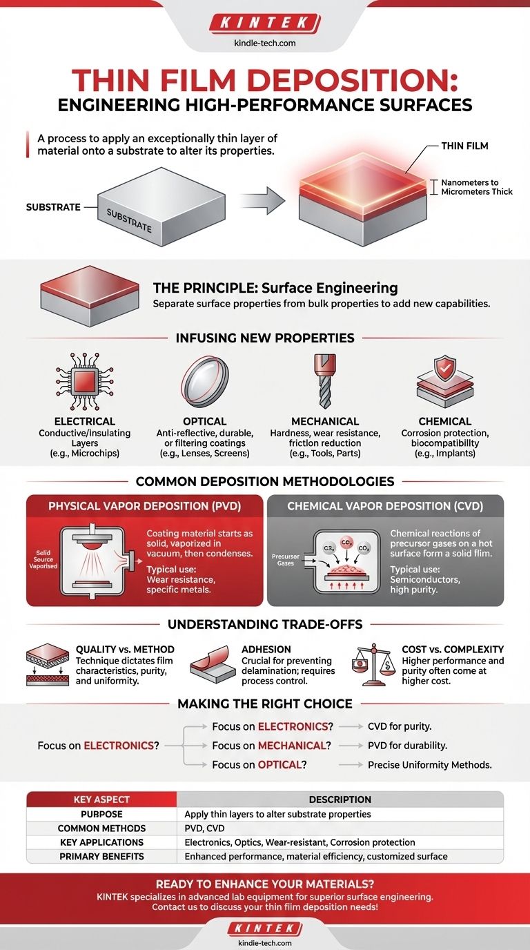
At its core, thin film deposition is a manufacturing process used to apply an exceptionally thin layer of material onto a surface, known as a substrate. These films, often just a few nanometers to micrometers thick, are not merely cosmetic; they are engineered to fundamentally alter the substrate's physical, chemical, or electrical properties to improve its performance for a specific application.
The true power of thin film deposition lies in its ability to separate a material's surface properties from its bulk properties. This allows us to create components that possess the ideal core characteristics (like strength or cost-effectiveness) while exhibiting entirely different, highly engineered behaviors on the surface.
The Principle: Engineering a High-Performance Surface
The fundamental goal of thin film deposition is to add new capabilities to a material that it does not inherently possess. Instead of making an entire object out of an expensive, conductive, or corrosion-resistant material, we can use a cheaper or stronger base and simply add a high-performance surface layer.
What Qualifies as a "Thin Film"?
A thin film is a layer of material ranging from a few atoms thick (nanometers) up to several micrometers. For perspective, this is often hundreds or even thousands of times thinner than a human hair. This microscopic scale is where materials can exhibit unique optical and electrical properties not seen in their bulk form.
The Goal: Infusing New Properties
By depositing a specific material, we can precisely control and enhance the substrate's characteristics. This is done to achieve a targeted outcome.
- Electrical Properties: Films can be used to add conductive pathways on an insulating substrate (like in microchips) or to add an insulating layer onto a conductive one.
- Optical Properties: The process can create anti-reflective coatings on lenses, make glass for screens more durable, or filter specific wavelengths of light.
- Mechanical Properties: Coatings add hardness and wear resistance to cutting tools, reduce friction on moving parts, and improve fatigue life.
- Chemical Properties: A thin film can form a barrier that protects a metal from corrosion or makes a medical implant biocompatible with the human body.
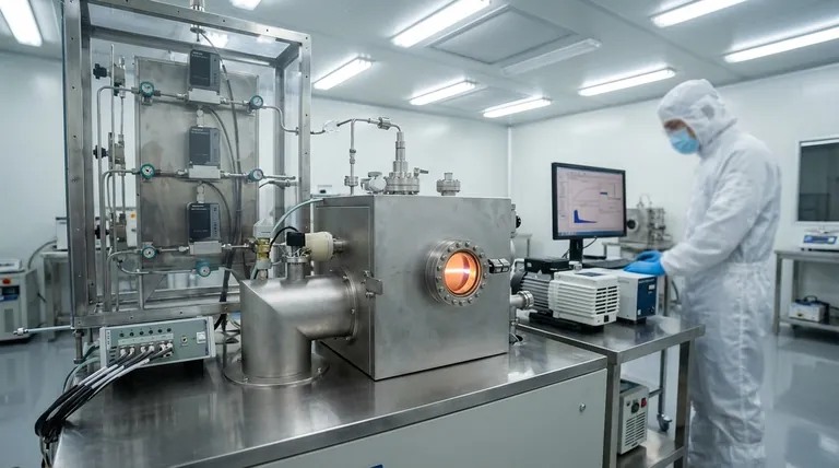
Common Deposition Methodologies
While there are many specific techniques, they generally fall into two major categories. The choice of method is critical as it dictates the film's quality, the materials that can be used, and the overall cost.
Physical Vapor Deposition (PVD)
In PVD, the coating material starts as a solid. It is then vaporized in a vacuum environment using physical means, such as heating it until it evaporates or bombarding it with ions (a process called sputtering). This vapor then travels and condenses onto the substrate, forming a thin, solid film.
Chemical Vapor Deposition (CVD)
CVD uses chemical reactions to create the film. Precursor gases are introduced into a reaction chamber containing the heated substrate. These gases react or decompose on the hot surface, leaving behind a solid film of the desired material. This method is essential for creating the highly pure, crystalline films required in semiconductor manufacturing.
Understanding the Trade-offs
Thin film deposition is a powerful but complex process. The success of an application depends on navigating the inherent trade-offs between cost, performance, and material compatibility.
Method Dictates Quality
The deposition technique directly impacts the film's final characteristics. PVD might be faster and more versatile for certain metals, while CVD often produces films with higher purity and better structural uniformity, which is critical for electronics.
Adhesion is Not Guaranteed
A primary challenge is ensuring the deposited film adheres strongly to the substrate. Poor adhesion can lead to delamination and complete failure of the component. Surface preparation and process control are paramount.
Cost vs. Complexity
Simple protective coatings for tools may be relatively inexpensive to apply. However, the multi-layer, ultra-pure films used in semiconductors and advanced optics require sophisticated equipment and cleanroom environments, making the process significantly more costly.
Making the Right Choice for Your Goal
The optimal deposition strategy is entirely dependent on the end-use application and performance requirements.
- If your primary focus is advanced electronics: You require the extreme purity and structural perfection achieved through methods like CVD to create reliable semiconductor devices.
- If your primary focus is mechanical durability: You need a hard, dense coating with excellent adhesion, often applied with specific PVD techniques to protect tools and engine parts from wear.
- If your primary focus is optical performance: Your goal is precise control over thickness and refractive index to create lenses and sensors, which demands highly uniform deposition methods.
Ultimately, thin film deposition empowers us to design materials not for what they are, but for what we need their surface to do.
Summary Table:
| Key Aspect | Description |
|---|---|
| Purpose | Apply thin layers (nanometers to micrometers) to alter substrate properties |
| Common Methods | Physical Vapor Deposition (PVD), Chemical Vapor Deposition (CVD) |
| Key Applications | Electronics, optics, wear-resistant coatings, corrosion protection |
| Primary Benefits | Enhanced performance, material efficiency, customized surface properties |
Ready to enhance your materials with precision thin film deposition? KINTEK specializes in advanced lab equipment and consumables for thin film applications, helping laboratories achieve superior surface engineering results. Whether you're developing semiconductors, optical coatings, or durable mechanical components, our expertise ensures optimal adhesion, purity, and performance. Contact us today to discuss how our solutions can meet your specific deposition needs!
Visual Guide
Related Products
- Aluminized Ceramic Evaporation Boat for Thin Film Deposition
- Tungsten Evaporation Boat for Thin Film Deposition
- Electron Beam Evaporation Coating Oxygen-Free Copper Crucible and Evaporation Boat
- Molybdenum Tungsten Tantalum Evaporation Boat for High Temperature Applications
- Vacuum Hot Press Furnace Machine for Lamination and Heating
People Also Ask
- Why are high-purity ceramic boats used for lignin activation? Ensure Purity & Thermal Stability
- What are thin films deposited by evaporation? A Guide to High-Purity Coating
- What is the widely used boat made of in thermal evaporation? Choosing the Right Material for High-Purity Deposition
- Why is an alumina boat and Ti3AlC2 powder bed necessary for Ti2AlC sintering? Protect MAX Phase Purity
- What are the applications of thin films deposition? Unlock New Possibilities for Your Materials


