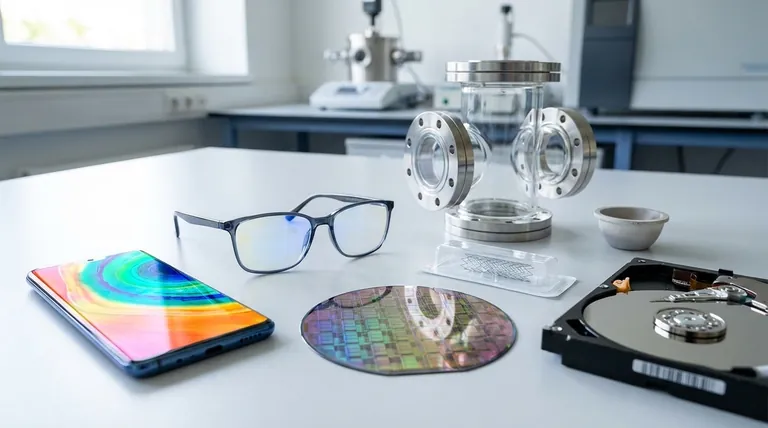
At its core, thin film deposition is a foundational manufacturing process used to apply a microscopic layer of material onto a surface. This technology is the invisible engine behind modern life, enabling everything from the anti-glare coating on your eyeglasses and the screen on your smartphone to advanced medical implants and the powerful processors inside our computers.
The true value of thin film deposition is not simply in applying a coating, but in fundamentally changing the properties of a material's surface. It allows us to grant an ordinary object extraordinary capabilities—like conductivity, durability, or specific optical behaviors—without altering its core structure.
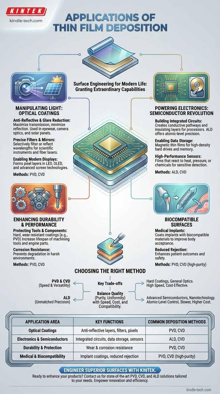
Manipulating Light: The World of Optical Coatings
One of the most widespread applications of thin film deposition is in controlling how light interacts with a surface. By precisely controlling the thickness and composition of these films, we can engineer specific optical outcomes.
Improving Transmission and Reducing Glare
Anti-reflective coatings on lenses, camera optics, and solar panels are created using thin films. These layers are designed to minimize light reflection, which maximizes the light that passes through, improving clarity and efficiency.
Creating Precise Filters and Mirrors
Thin films are essential for creating devices that filter or reflect specific wavelengths of light. This is critical for scientific instruments, fiber lasers, and the specialized mirrors used in telescopes and other precision optics.
Enabling Modern Displays
The vibrant colors on LED, OLED, and other advanced displays are a direct result of thin film deposition. The process is used to build up the microscopic layers of light-emitting or light-absorbing materials that form each individual pixel.
Powering Electronics: The Semiconductor Revolution
The entire semiconductor industry is built upon thin film deposition. The process allows for the creation of the incredibly complex, layered structures that make up integrated circuits, memory, and processors.
Building Integrated Circuits
In a microchip, thin films create the conductive pathways for electricity and the insulating layers that prevent short circuits. Techniques like Atomic Layer Deposition (ALD) allow for films to be deposited one atomic layer at a time, enabling the creation of today's ultra-small and powerful transistors.
Enabling Data Storage
The magnetic layers on hard disk drives and other data storage media are deposited as thin films. The properties of this film determine the density and reliability of the data storage.
Fabricating High-Performance Sensors
Thin film deposition is also used to create a wide variety of sensors. By depositing materials that change their electrical properties in response to heat, pressure, or specific chemicals, we can create compact and highly sensitive detection devices.
Enhancing Durability and Performance
Beyond optics and electronics, thin films are used to give materials new physical properties, such as hardness, corrosion resistance, and biocompatibility.
Protecting Tools and Components
Machining tools, engine parts, and other industrial components are often coated with hard, wear-resistant thin films using methods like Physical Vapor Deposition (PVD). This dramatically increases their lifespan and performance under extreme conditions.
Creating Biocompatible Surfaces
Medical implants, such as artificial joints or stents, are coated with thin films of biocompatible material. This coating helps the body accept the implant, reducing the risk of rejection and improving patient outcomes.
Understanding the Trade-offs: Choosing the Right Method
The term "thin film deposition" covers several different techniques, and the choice of method is a critical engineering decision based on the desired outcome and economic realities.
The Speed and Versatility of PVD & CVD
Physical Vapor Deposition (PVD) and Chemical Vapor Deposition (CVD) are the workhorses of the industry. They are relatively fast and cost-effective, making them ideal for applying hard coatings to tools or general optical coatings where atomic-level perfection is not required.
The Unmatched Precision of ALD
Atomic Layer Deposition (ALD) offers unparalleled control, depositing films with perfect uniformity one atomic layer at a time. This precision is essential for modern, high-performance semiconductors but comes at the cost of being a much slower and more expensive process.
The Need for a Balanced Approach
No single method is universally superior. The decision always involves a trade-off between the required film quality—its purity, thickness uniformity, and structure—and the practical constraints of production speed, equipment cost, and material compatibility.
Making the Right Choice for Your Application
To select the right approach, you must first define the most critical property your surface needs.
- If your primary focus is high-performance optics: You need a deposition method that offers precise control over film thickness and refractive index.
- If your primary focus is advanced semiconductors: Atomic-level precision is non-negotiable, meaning techniques like ALD are often essential.
- If your primary focus is mechanical durability: Cost-effective and robust methods like PVD or CVD are typically the most practical choice for applying hard coatings.
- If your primary focus is biocompatibility: The purity of the deposited material is paramount, and the chosen method must ensure no contaminants are introduced.
Ultimately, thin film deposition is about engineering surfaces to unlock new possibilities for the materials we use every day.
Summary Table:
| Application Area | Key Functions | Common Deposition Methods |
|---|---|---|
| Optical Coatings | Anti-reflective layers, precise filters, display pixels | PVD, CVD |
| Electronics & Semiconductors | Integrated circuits, data storage, sensors | ALD, CVD |
| Durability & Protection | Wear-resistant coatings, corrosion resistance | PVD, CVD |
| Medical & Biocompatibility | Implant coatings for reduced rejection | PVD, CVD (high-purity) |
Ready to Engineer Superior Surfaces for Your Products?
Thin film deposition is the key to unlocking enhanced performance, whether you need precise optical coatings, durable protective layers, or advanced semiconductor components. At KINTEK, we specialize in providing state-of-the-art lab equipment and consumables tailored to your deposition needs—from cost-effective PVD/CVD systems to high-precision ALD solutions.
Let our experts help you select the right method to achieve the perfect balance of quality, speed, and cost for your application. Contact us today to discuss how KINTEK can empower your laboratory's innovation and efficiency!
Visual Guide
Related Products
- Aluminized Ceramic Evaporation Boat for Thin Film Deposition
- Tungsten Evaporation Boat for Thin Film Deposition
- Electron Beam Evaporation Coating Oxygen-Free Copper Crucible and Evaporation Boat
- Molybdenum Tungsten Tantalum Evaporation Boat for High Temperature Applications
- Vacuum Hot Press Furnace Machine for Lamination and Heating
People Also Ask
- What is the widely used boat made of in thermal evaporation? Choosing the Right Material for High-Purity Deposition
- What are the alternatives to sputtering? Choose the Right Thin Film Deposition Method
- What are thin films deposited by evaporation? A Guide to High-Purity Coating
- Why is an alumina boat selected for catalyst precursors? Ensure Sample Purity at 1000 °C
- Why is an alumina boat and Ti3AlC2 powder bed necessary for Ti2AlC sintering? Protect MAX Phase Purity


