At its core, Plasma-Enhanced Chemical Vapor Deposition (PECVD) is a foundational technology for manufacturing the micro-scale devices that power our modern world. Its primary applications are in fabricating semiconductor integrated circuits, optoelectronic devices like solar cells and LEDs, and Micro-Electro-Mechanical Systems (MEMS). PECVD is specifically used to deposit thin, functional layers of material—such as insulators, protective coatings, or optical films—onto a substrate.
The central value of PECVD lies in its ability to deposit high-quality, uniform films at low temperatures. This single characteristic allows it to add critical layers to complex, delicate devices without damaging the sensitive structures already built on the substrate.
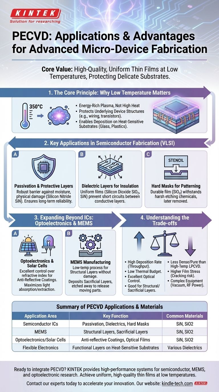
The Core Principle: Why Low Temperature is Crucial
The defining advantage of PECVD over other deposition methods is its use of an energy-rich plasma rather than high heat to drive chemical reactions. This allows for processing at significantly lower temperatures, typically around 350°C.
Protecting Underlying Device Structures
Modern microchips are built layer by layer, with intricate metal wiring and sensitive transistors. High-temperature processes, often exceeding 600°C, would melt the aluminum or copper interconnects and destroy the delicate device architecture fabricated in previous steps. PECVD's low-temperature nature makes it a "back-end-of-line" compatible process, meaning it can be safely performed on nearly completed wafers.
Enabling a Wider Range of Substrates
The low thermal budget of PECVD also allows for deposition on materials that cannot withstand high heat. This includes certain types of glass, plastics, and flexible substrates, expanding its use beyond traditional silicon wafers.
Key Applications in Semiconductor Fabrication
In Very Large Scale Integration (VLSI) circuits, PECVD is a workhorse process used to create several types of essential films. The quality, uniformity, and conformality (step coverage) of these films are critical for device performance and reliability.
Passivation and Protective Layers
The final step in creating many chips is to encapsulate them in a protective layer. PECVD is used to deposit films like silicon nitride (SiN), which act as a robust barrier against moisture, mobile ions, and physical damage, ensuring the long-term reliability of the integrated circuit.
Dielectric Layers for Insulation
Circuits contain multiple levels of metal wiring that must be electrically isolated from one another. PECVD deposits uniform films of silicon dioxide (SiO2) or silicon nitride to serve as these inter-metal dielectrics, preventing short circuits between conductive layers.
Hard Masks for Patterning
To etch a precise pattern into a substrate, a durable stencil, or hard mask, is often required. PECVD can deposit a tough film (like SiO2) that can withstand the harsh etching chemicals used to pattern the underlying layer. This PECVD film is later removed.
Expanding Applications Beyond Integrated Circuits
The unique capabilities of PECVD make it essential for other advanced manufacturing fields.
Optoelectronics and Solar Cells
In devices that manage light, controlling optical properties is paramount. PECVD offers excellent control over a film's refractive index, making it the ideal method for depositing anti-reflective coatings on solar cells and LEDs. This maximizes light absorption (in solar cells) or extraction (in LEDs), directly improving efficiency.
MEMS Manufacturing
Micro-Electro-Mechanical Systems (MEMS) combine tiny mechanical components with electronics. PECVD's low-temperature process is ideal for building the structural layers of these devices without damaging sensitive components. It is also used to deposit sacrificial layers, which provide a temporary scaffold during fabrication and are later etched away to release moving parts.
Understanding the Trade-offs
While powerful, PECVD is not a universal solution. Choosing a deposition technology requires understanding its limitations.
Film Quality vs. Deposition Temperature
PECVD films are high-quality, but they are generally less dense and pure than films deposited at higher temperatures using methods like Low-Pressure CVD (LPCVD). The plasma process can incorporate elements like hydrogen into the film, which can sometimes negatively impact device performance.
Deposition Rate vs. Film Stress
PECVD typically offers a much higher deposition rate than LPCVD, which is a significant advantage for manufacturing throughput. However, these rapidly deposited films can have higher internal stress, which may lead to cracking or delamination if not properly managed.
Process and Equipment Complexity
A PECVD system requires a vacuum chamber, gas delivery systems, and a radio-frequency (RF) power source to generate the plasma. This makes the equipment more complex and costly than simpler atmospheric pressure deposition methods.
Making the Right Choice for Your Goal
Selecting a deposition method depends entirely on the priorities of your specific application and the constraints of your substrate.
- If your primary focus is throughput on temperature-sensitive substrates: PECVD is almost always the superior choice due to its high deposition rate and low thermal budget.
- If your primary focus is the absolute highest film purity and density: A higher-temperature process like LPCVD may be required, provided your substrate can withstand the heat.
- If your primary focus is creating precise optical films: PECVD is the clear winner because of its excellent control over refractive index.
- If your primary focus is creating thick structural or sacrificial layers for MEMS: PECVD's high deposition rate and low-stress film options make it a go-to technology.
Ultimately, understanding these trade-offs allows you to select the deposition technique that best aligns with your device requirements and manufacturing goals.
Summary Table:
| Application Area | Key Function of PECVD | Common Materials Deposited |
|---|---|---|
| Semiconductor ICs | Passivation, Inter-metal Dielectrics, Hard Masks | Silicon Nitride (SiN), Silicon Dioxide (SiO2) |
| MEMS | Structural Layers, Sacrificial Layers | Silicon Nitride, Silicon Dioxide |
| Optoelectronics/Solar Cells | Anti-reflective Coatings, Optical Films | Silicon Nitride, Silicon Dioxide |
| Flexible Electronics | Functional Layers on Heat-Sensitive Substrates | Various dielectrics and protective coatings |
Ready to integrate PECVD into your lab's workflow?
KINTEK specializes in providing high-performance lab equipment and consumables, including advanced PECVD systems tailored for semiconductor, MEMS, and optoelectronic research and production. Our solutions help you achieve uniform, high-quality thin films at low temperatures, protecting your delicate substrates and enhancing device performance.
Contact our experts today to discuss how our PECVD technology can meet your specific application needs and accelerate your innovation.
Visual Guide
Related Products
- Inclined Rotary Plasma Enhanced Chemical Vapor Deposition PECVD Equipment Tube Furnace Machine
- Chemical Vapor Deposition CVD Equipment System Chamber Slide PECVD Tube Furnace with Liquid Gasifier PECVD Machine
- Inclined Rotary Plasma Enhanced Chemical Vapor Deposition PECVD Equipment Tube Furnace Machine
- RF PECVD System Radio Frequency Plasma-Enhanced Chemical Vapor Deposition RF PECVD
- Multi Heating Zones CVD Tube Furnace Machine Chemical Vapor Deposition Chamber System Equipment
People Also Ask
- What are the core advantages of PE-CVD in OLED encapsulation? Protect Sensitive Layers with Low-Temp Film Deposition
- What is the necessity of depositing a silicon nitride (SiNx) thin film using PECVD? Optimize QSSPC Lifetime Measurement
- How does PECVD equipment facilitate the directional growth of carbon nanotubes? Achieve Precision Vertical Alignment
- What are the advantages of plasma enhanced chemical vapor deposition? Enable Low-Temperature, High-Quality Film Deposition
- What is plasma enhanced chemical vapor deposition PECVD equipment? A Guide to Low-Temperature Thin Film Deposition


