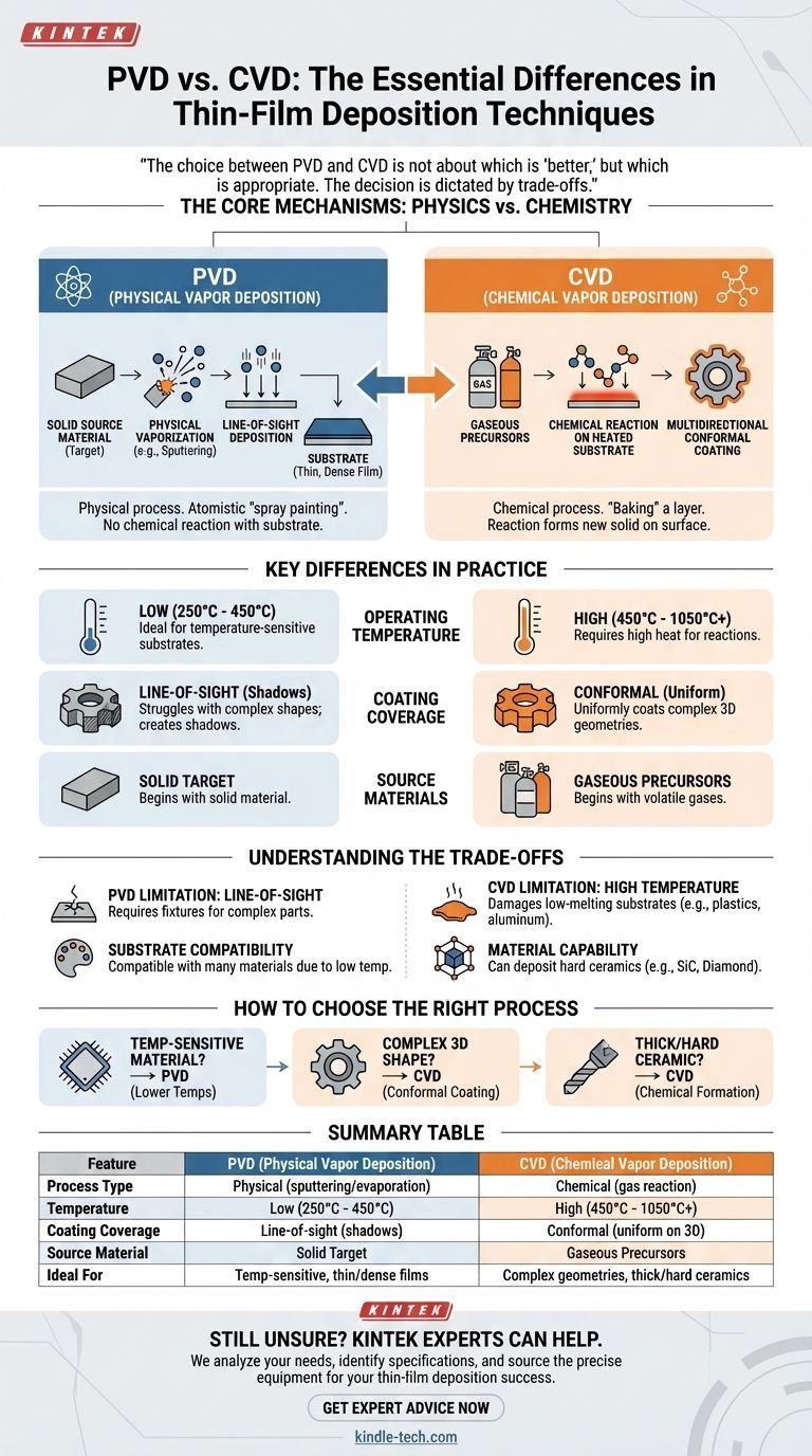
The fundamental distinction between PVD and CVD lies in the state of the material and the nature of the deposition. Physical Vapor Deposition (PVD) is a physical process that turns a solid material into a vapor, which then condenses onto a substrate. In contrast, Chemical Vapor Deposition (CVD) is a chemical process where precursor gases react on a heated substrate surface to form a new, solid film.
The choice between PVD and CVD is not about which is "better," but which is appropriate. The decision is dictated by the trade-offs between operating temperature, the geometry of the part being coated, and the specific properties required of the final film.
The Core Mechanisms: Physics vs. Chemistry
To select the right method, you must first understand how each process works at a fundamental level. One is a process of physical transformation, while the other relies on creating something new through chemical reaction.
How PVD Works (A Physical Process)
PVD is essentially a high-tech "spray painting" process using atoms. It begins with a solid source material, often called a target.
This solid target is bombarded with energy (like an ion beam) inside a vacuum chamber, causing atoms or molecules to be ejected from its surface.
This vaporized material then travels in a straight line—a "line-of-sight" path—and condenses on the cooler substrate, forming a thin, solid film. No chemical reaction occurs with the substrate itself.
How CVD Works (A Chemical Process)
CVD is more like baking a layer onto a surface. It begins with one or more volatile precursor gases that are introduced into a reaction chamber.
The substrate within the chamber is heated to a high temperature, which provides the energy needed to trigger a chemical reaction between the gases.
This reaction causes a new, non-volatile solid material to form and deposit onto the heated substrate. Because the deposition happens from a gas phase, it is multidirectional, coating all exposed surfaces uniformly.
Key Differences in Practice
The differences in their core mechanisms lead to significant practical distinctions in temperature, the resulting coating, and the materials involved.
Operating Temperature
This is often the most critical deciding factor. PVD operates at relatively low temperatures, typically between 250°C and 450°C.
CVD, however, requires much higher temperatures to drive the necessary chemical reactions, usually ranging from 450°C to over 1050°C.
Coating Properties and Coverage
PVD's line-of-sight nature produces exceptionally thin, smooth, and dense coatings. However, it struggles to coat complex internal surfaces or the undersides of objects uniformly.
CVD's gas-based, multidirectional process provides a highly conformal coating, meaning it uniformly covers complex shapes, sharp corners, and internal geometries. These films can be made much thicker but may be rougher than PVD coatings.
Source Materials
The starting point for each process is fundamentally different. PVD always begins with a solid target of the material you wish to deposit.
CVD begins with gaseous precursor molecules. These gases contain the elements that will react and combine to form the final desired coating material on the substrate.
Understanding the Trade-offs
Neither technology is a universal solution. Understanding their inherent limitations is crucial for making an informed decision.
The Temperature Limitation of CVD
The high heat required for CVD is its greatest constraint. It makes the process unsuitable for substrates that have low melting points or could be damaged by thermal stress, such as plastics, aluminum alloys, or tempered steels.
The "Line-of-Sight" Limitation of PVD
The primary drawback of PVD is its inability to uniformly coat complex, three-dimensional parts. Areas not in the direct path of the vapor source will receive little to no coating, creating a "shadowing" effect. This often requires complex fixtures to rotate parts during deposition.
Substrate and Material Compatibility
The choice of substrate severely limits the use of CVD. PVD, with its lower temperatures, is compatible with a much wider range of substrate materials. Conversely, CVD can deposit certain materials (like diamond or silicon carbide) that are extremely difficult or impossible to create via PVD.
How to Choose the Right Process
To make a definitive choice, evaluate your primary technical requirement.
- If your primary focus is coating a temperature-sensitive material: PVD is the clear choice due to its significantly lower processing temperatures.
- If your primary focus is achieving a uniform coating on a complex 3D shape: CVD is superior due to its conformal, gas-based deposition.
- If your primary focus is creating an extremely hard, thick, or specific ceramic coating (like SiC): CVD is often the only viable technology, provided your substrate can withstand the heat.
By understanding these core principles, you can select the deposition technology that aligns perfectly with your material, geometry, and performance goals.
Summary Table:
| Feature | PVD (Physical Vapor Deposition) | CVD (Chemical Vapor Deposition) |
|---|---|---|
| Process Type | Physical (sputtering/evaporation) | Chemical (gas reaction) |
| Temperature | Low (250°C - 450°C) | High (450°C - 1050°C+) |
| Coating Coverage | Line-of-sight (shadows complex shapes) | Conformal (uniform on 3D parts) |
| Source Material | Solid Target | Gaseous Precursors |
| Ideal For | Temperature-sensitive substrates, thin/dense films | Complex geometries, thick/hard ceramic coatings |
Still Unsure Which Coating Process is Right for Your Application?
Selecting between PVD and CVD is critical for achieving the desired performance, durability, and quality in your lab equipment or components. KINTEK specializes in providing the right laboratory equipment and consumables to meet your specific thin-film deposition needs.
Our experts can help you:
- Analyze your substrate material and geometry to determine the optimal process.
- Identify the coating specifications required for your application's success.
- Source the precise equipment and materials you need for reliable, repeatable results.
Don't let the wrong choice compromise your project. Contact our technical team today for a personalized consultation and ensure your deposition process is a success.
Visual Guide
Related Products
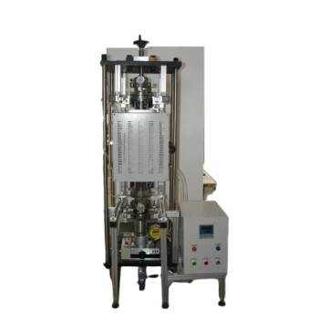
- Customer Made Versatile CVD Tube Furnace Chemical Vapor Deposition Chamber System Equipment
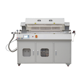
- Split Chamber CVD Tube Furnace with Vacuum Station Chemical Vapor Deposition System Equipment Machine
- 1200℃ Split Tube Furnace with Quartz Tube Laboratory Tubular Furnace
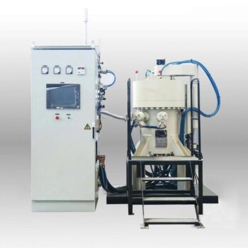
- Vacuum Hot Press Furnace Heated Vacuum Press Machine Tube Furnace
- Vacuum Heat Treat Sintering Brazing Furnace
People Also Ask
- How do nanotubes affect the environment? Balancing Low Carbon Footprint with Ecological Risks
- How high of temperature do carbon nanotubes in air have the ability to sustain? Understanding the Oxidation Limit
- What are the challenges of carbon nanotubes? Overcoming Production and Integration Hurdles
- What is a CVD tube furnace? A Complete Guide to Thin-Film Deposition
- Why are carbon nanotubes important in industry? Unlocking Next-Generation Material Performance