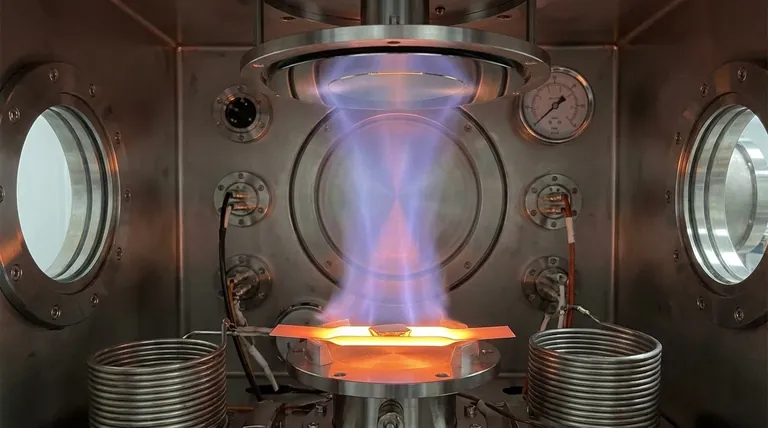
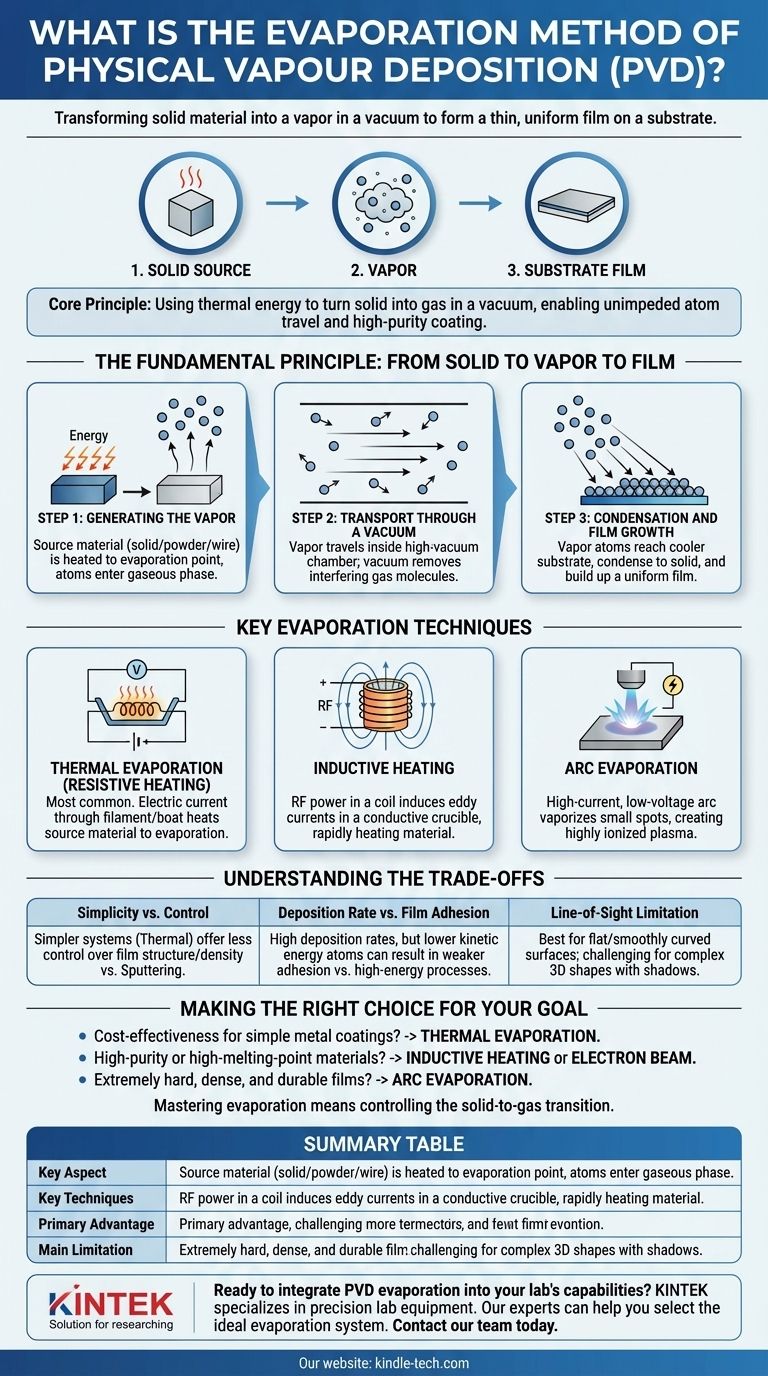
In physical vapor deposition (PVD), the evaporation method is a family of processes where a source material is heated in a vacuum chamber until it transforms into a vapor. This vapor then travels through the vacuum and condenses onto a cooler surface, known as the substrate, forming a thin, uniform film.
The core principle is simple: use thermal energy to turn a solid material into a gas within a vacuum. This allows its atoms to travel unimpeded and deposit onto a target surface, creating a high-purity coating.
The Fundamental Principle: From Solid to Vapor to Film
The entire process is governed by a straightforward, three-step sequence that takes place under controlled vacuum conditions.
Step 1: Generating the Vapor
The process begins by supplying energy to a source material, often in the form of a solid block, powder, or wire. This energy heats the material to its evaporation point, causing its atoms to break free from the surface and enter a gaseous phase.
Step 2: Transport Through a Vacuum
This vapor phase occurs inside a high-vacuum chamber. The vacuum is critical because it removes air and other gas molecules that would otherwise collide with the vapor atoms, scattering them and introducing impurities. In a vacuum, the vapor atoms travel in a straight, line-of-sight path from the source to the substrate.
Step 3: Condensation and Film Growth
When the vapor atoms reach the cooler substrate, they lose energy and condense back into a solid state. They adhere to the surface and gradually build up, atom by atom, to form a thin, solid film with the same chemical composition as the source material.
Key Evaporation Techniques
While the principle remains the same, different methods are used to supply the energy required for evaporation. The choice of technique depends on the material being deposited and the desired film properties.
Thermal Evaporation (Resistive Heating)
This is the most common and direct method. An electric current is passed through a high-resistance filament or "boat" (often made of tungsten or molybdenum) that holds the source material. The boat heats up, transferring thermal energy to the material and causing it to evaporate.
Inductive Heating
In this technique, a crucible containing the source material is placed inside a coil. A high-frequency alternating current (RF power) is run through the coil, which generates a changing magnetic field. This field induces eddy currents within the conductive crucible, causing it to heat up rapidly and evaporate the material inside.
Arc Evaporation
This is a higher-energy process used for creating very hard and dense films. A high-current, low-voltage electric arc is ignited on the surface of the solid source target. The intense energy of the arc vaporizes small spots of the material, creating a highly ionized vapor, or plasma, which is then directed toward the substrate.
Understanding the Trade-offs
Evaporation is a powerful PVD method, but it's important to understand its characteristics compared to other techniques like sputtering.
Simplicity vs. Control
Evaporation systems, particularly thermal evaporation, are often simpler and less expensive to operate. However, they can offer less control over the film's structure and density compared to sputtering.
Deposition Rate vs. Film Adhesion
Evaporation can achieve very high deposition rates, making it efficient for some applications. However, because the vapor atoms arrive with relatively low kinetic energy, the adhesion of the film to the substrate can sometimes be weaker than films produced by higher-energy processes like arc evaporation or sputtering.
Line-of-Sight Limitation
Because the vapor travels in a straight line, evaporation is best suited for coating flat or smoothly curved surfaces. It can be challenging to achieve a uniform coating on complex, three-dimensional shapes with shadowed areas.
Making the Right Choice for Your Goal
Selecting the appropriate evaporation technique is a matter of matching the process capabilities to your specific requirements for the material and the final film.
- If your primary focus is cost-effectiveness for simple metal coatings: Thermal (resistive) evaporation is often the ideal choice due to its simplicity and high deposition rates.
- If your primary focus is depositing high-purity or high-melting-point materials: Inductive heating or electron beam evaporation (a related technique) provides the necessary energy without direct contact from a heating element.
- If your primary focus is creating extremely hard, dense, and durable films: Arc evaporation is superior, as the plasma it generates results in a more robust and adherent coating.
Ultimately, mastering the evaporation method means understanding that you are simply controlling the transition of matter from a solid to a gas and back again.
Summary Table:
| Key Aspect | Description |
|---|---|
| Core Principle | Heating a solid source material in a vacuum until it vaporizes and condenses on a substrate. |
| Key Techniques | Thermal (Resistive), Inductive (RF), Arc Evaporation. |
| Primary Advantage | High deposition rates and high-purity films. |
| Main Limitation | Line-of-sight deposition, less suitable for complex 3D shapes. |
Ready to integrate PVD evaporation into your lab's capabilities? KINTEK specializes in precision lab equipment and consumables. Our experts can help you select the ideal evaporation system—whether it's cost-effective thermal evaporation for simple coatings or advanced arc evaporation for durable films—to meet your specific research and production goals. Contact our team today to discuss your project and discover the KINTEK difference in laboratory performance.
Visual Guide
Related Products
- Chemical Vapor Deposition CVD Equipment System Chamber Slide PECVD Tube Furnace with Liquid Gasifier PECVD Machine
- Customer Made Versatile CVD Tube Furnace Chemical Vapor Deposition Chamber System Equipment
- RF PECVD System Radio Frequency Plasma-Enhanced Chemical Vapor Deposition RF PECVD
- 915MHz MPCVD Diamond Machine Microwave Plasma Chemical Vapor Deposition System Reactor
- HFCVD Machine System Equipment for Drawing Die Nano-Diamond Coating
People Also Ask
- What is the chemical vapor deposition growth process? Build Superior Thin Films from the Atom Up
- What happens during deposition chemistry? Building Thin Films from Gaseous Precursors
- What are the processes of vapor phase deposition? Understand CVD vs. PVD for Superior Thin Films
- How expensive is chemical vapor deposition? Understanding the True Cost of High-Performance Coating
- What types of substrates are used in CVD to facilitate graphene films? Optimize Graphene Growth with the Right Catalyst


