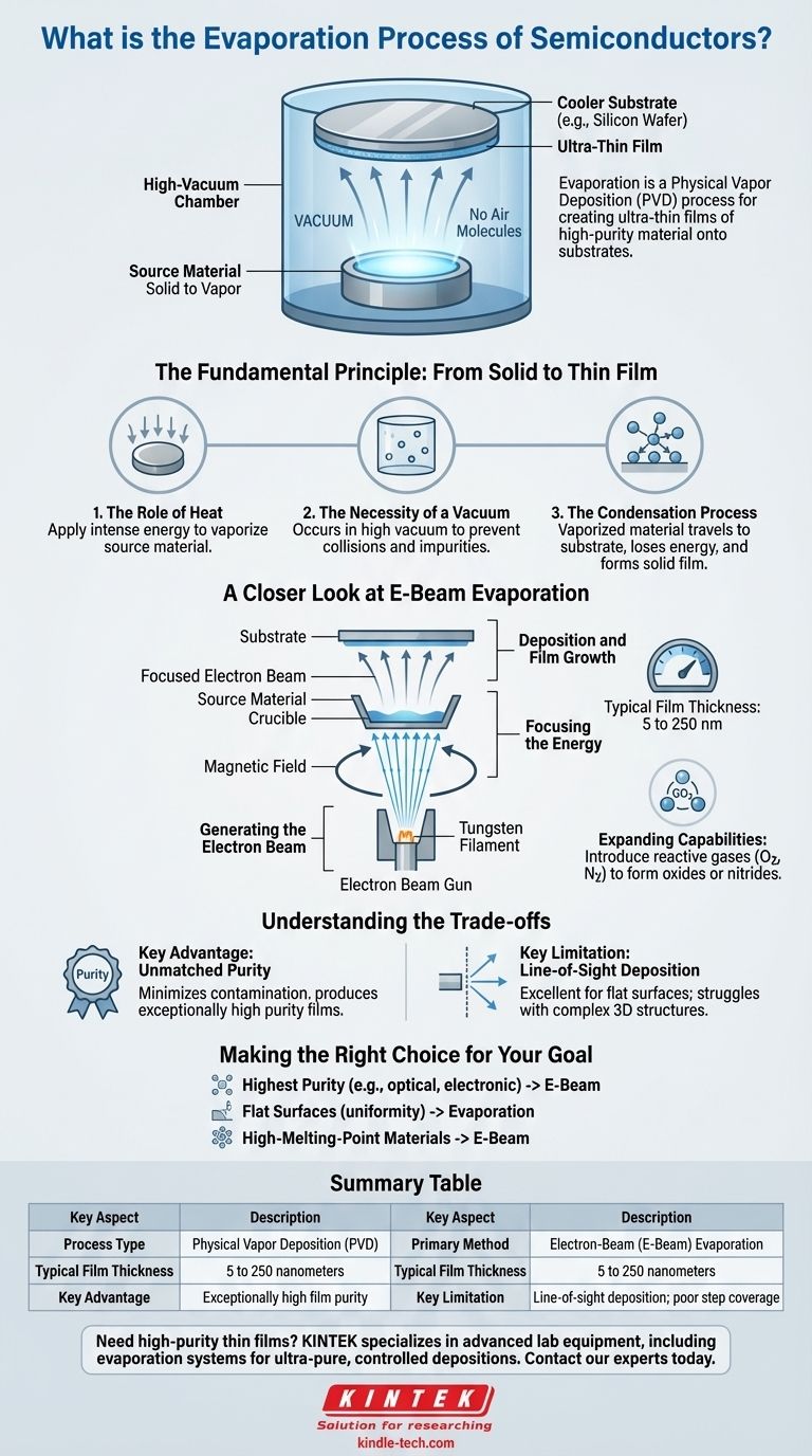
In the context of semiconductors, evaporation is a physical vapor deposition (PVD) process used to create ultra-thin films of a material onto a substrate, such as a silicon wafer. It involves heating a source material in a high-vacuum chamber until it turns into a gas. These gaseous atoms then travel through the vacuum and condense onto the cooler substrate, forming a solid, high-purity film.
The core principle of evaporation is using thermal energy in a vacuum to transform a solid material into a vapor, which then re-solidifies as a precisely controlled, thin layer on a target surface. This method is fundamental to building the intricate structures found in microprocessors and integrated circuits.
The Fundamental Principle: From Solid to Thin Film
At its heart, evaporation is a three-step process designed for atomic-level construction. Each step is critical for ensuring the quality and integrity of the final film.
The Role of Heat
The process begins by applying intense energy to a source material, often in the form of a small pellet or ingot. The goal is to raise the material's temperature to its vaporization point, causing it to evaporate (or sublimate, moving directly from solid to gas).
The Necessity of a Vacuum
This entire process occurs within a high-vacuum environment. The vacuum is crucial because it removes air and other gas molecules that would otherwise collide with the vaporized atoms, deflecting them or introducing impurities into the film.
The Condensation Process
With a clear, unobstructed path, the vaporized material travels directly to the substrate, which is strategically placed above the source. Upon contact with the cooler substrate surface, the atoms lose their thermal energy, condense, and bond to the surface, gradually building the desired thin film.
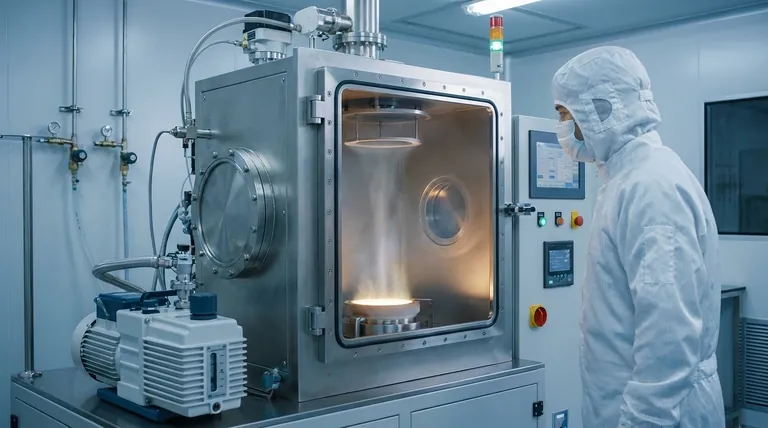
A Closer Look at E-Beam Evaporation
While several heating methods exist, electron-beam (e-beam) evaporation is a dominant technique in the semiconductor industry due to its precision and ability to handle a wide range of materials.
Generating the Electron Beam
The process starts with a tungsten filament that is heated to a high temperature, causing it to emit a stream of electrons. These electrons are then accelerated by a high-voltage field.
Focusing the Energy
A powerful magnetic field is used to guide and focus these high-energy electrons into a tight beam. This beam is precisely directed at the source material held in a container called a crucible.
Deposition and Film Growth
The intense energy from the electron beam melts and then evaporates the source material. The resulting vapor flows upwards and deposits onto the substrate, creating a film of very high purity. The final coating thickness is tightly controlled, typically ranging from 5 to 250 nanometers.
Expanding Capabilities with Reactive Gases
The e-beam process can be adapted to create compounds. By introducing a reactive gas, such as oxygen or nitrogen, into the chamber during deposition, it's possible to form non-metallic films like metal oxides or nitrides on the wafer.
Understanding the Trade-offs
Evaporation is a powerful technique, but like any engineering process, it involves specific advantages and limitations that determine its suitability for a given application.
Key Advantage: Unmatched Purity
The primary benefit of e-beam evaporation is the ability to produce films with exceptionally high purity. Because only the source material is heated directly by the electron beam, contamination from the heating apparatus or crucible is minimal.
Key Limitation: Line-of-Sight Deposition
Evaporation is a directional, line-of-sight process. Atoms travel in a straight line from the source to the substrate. This means it is excellent for coating flat surfaces but struggles to evenly coat complex, three-dimensional structures with undercuts or trenches.
Making the Right Choice for Your Goal
Selecting the right deposition method depends entirely on the specific requirements of the film and the device being manufactured.
- If your primary focus is achieving the highest possible film purity: E-beam evaporation is often the superior choice, especially for sensitive optical or electronic layers.
- If you are depositing a film on a relatively flat surface: Evaporation provides excellent uniformity and control for simple geometries.
- If you need to deposit high-melting-point metals or certain dielectrics: The focused energy of an electron beam makes it one of the few methods capable of vaporizing these robust materials effectively.
Evaporation is a foundational technology that enables the precise layering required to construct the complex world of modern microelectronics.
Summary Table:
| Key Aspect | Description |
|---|---|
| Process Type | Physical Vapor Deposition (PVD) |
| Primary Method | Electron-Beam (E-Beam) Evaporation |
| Typical Film Thickness | 5 to 250 nanometers |
| Key Advantage | Exceptionally high film purity |
| Key Limitation | Line-of-sight deposition; poor step coverage |
Need high-purity thin films for your semiconductor R&D or production?
KINTEK specializes in advanced lab equipment, including evaporation systems, to meet the precise demands of semiconductor fabrication. Our solutions help you achieve the ultra-pure, controlled depositions critical for building next-generation microprocessors and integrated circuits.
Contact our experts today to discuss how our evaporation technology can enhance your laboratory's capabilities.
Visual Guide
Related Products
- Electron Beam Evaporation Coating Gold Plating Tungsten Molybdenum Crucible for Evaporation
- Electron Beam Evaporation Coating Tungsten Crucible and Molybdenum Crucible for High Temperature Applications
- Electron Beam Evaporation Coating Oxygen-Free Copper Crucible and Evaporation Boat
- Hemispherical Bottom Tungsten Molybdenum Evaporation Boat
- High Purity Pure Graphite Crucible for Electron Beam Evaporation
People Also Ask
- What are the applications of e-beam evaporation? Achieve High-Purity Coatings for Optics & Electronics
- What is e-beam evaporation used for? Precision Coating for Optics, Aerospace & Electronics
- What is the process of e-beam coating? Achieve High-Purity, Precise Thin Films for Your Lab
- What is the temperature of e-beam evaporation? Mastering the Two-Zone Thermal Process for Precision Films
- What is the voltage of e-beam evaporation? Achieve Precise Thin-Film Deposition


