Crucially, there is no single universal formula for the deposition rate of a thin film. The specific equation used to calculate or model the rate is entirely dependent on the deposition method employed, such as Physical Vapor Deposition (PVD) or Chemical Vapor Deposition (CVD). Each technique is governed by different physical or chemical principles, and therefore, by a different set of mathematical relationships and controlling variables.
The core principle to understand is that deposition rate is not a fixed constant but a dynamic outcome of a system's specific parameters. The "formula" is a model describing how variables like source material flux, temperature, pressure, and system geometry interact to determine the film's growth speed.
The Fundamental Concept of Deposition Rate
The deposition rate (R) is fundamentally a measure of how quickly a film grows on a substrate. It is typically expressed as thickness per unit of time.
Defining the Rate
The most common units are nanometers per minute (nm/min), nanometers per second (nm/s), or angstroms per minute (Å/min). It is a critical parameter for controlling the final thickness and properties of the film.
Key Influencing Factors
While specific formulas vary, almost all deposition processes are influenced by a common set of physical factors. Understanding these factors is more important than memorizing a single equation.
- Source Flux: This is the rate at which atoms or molecules are generated from the source material. Higher flux generally leads to a higher deposition rate.
- Transport: This describes how the generated particles travel from the source to the substrate. In PVD, this is often line-of-sight travel in a vacuum, while in CVD, it involves gas flow and diffusion.
- Sticking Coefficient: This is the probability that a particle arriving at the substrate surface will successfully adhere and become part of the film. It is highly dependent on substrate temperature and material chemistry.
- System Geometry: The distance and angle between the source and the substrate have a direct impact. The rate typically decreases as the distance increases.
Rate Formulas for Common Deposition Methods
To illustrate how different the governing principles are, consider the conceptual models for two primary deposition categories: PVD and CVD.
Physical Vapor Deposition (PVD)
In PVD methods like sputtering or evaporation, a solid material is converted into a vapor phase and transported to the substrate.
For sputtering, the rate is primarily a function of the ion beam and target material properties. A simplified relationship is:
Rate ∝ (Ion Current Density) × (Sputter Yield)
Here, the sputter yield is the number of target atoms ejected per incident ion, a property unique to the target material and ion energy.
For thermal evaporation, the rate is governed by the vapor pressure of the source material (which is highly temperature-dependent) and the geometry of the system.
Chemical Vapor Deposition (CVD)
In CVD, precursor gases react on a heated substrate surface to form the film. The process can be limited by two different regimes.
- Mass-Transport-Limited Regime: At high temperatures, the reaction is so fast that the rate is limited only by how quickly reactant gases can be transported to the substrate surface.
- Surface-Reaction-Limited Regime: At lower temperatures, the rate is limited by the speed of the chemical reaction on the surface itself. This often follows an Arrhenius-type relationship, where the rate increases exponentially with temperature.
Understanding the Limitations and Real-World Complexities
A calculated theoretical deposition rate is only a starting point. Real-world processes are far more complex and require direct measurement for accurate control.
Theoretical vs. Actual Rates
Formulas provide an idealized model. In practice, factors like residual gas contamination, non-uniform temperature distribution, and evolving source conditions cause the actual rate to deviate from the theoretical one.
The Need for In-Situ Monitoring
Because of these complexities, most high-precision deposition systems do not rely on calculation alone. They use in-situ monitoring tools, like a Quartz Crystal Microbalance (QCM), which measures mass changes in real-time to provide an accurate, live reading of the deposition rate and film thickness.
The Problem of Uniformity
The deposition rate is rarely the same across the entire surface of the substrate. It is often highest directly in front of the source and decreases toward the edges. Achieving high uniformity is a major goal in thin film engineering.
How to Apply This to Your Goal
Your approach should be dictated by your specific objective, whether it's process control, system design, or theoretical understanding.
- If your primary focus is precise process control: Prioritize installing and calibrating an in-situ monitor like a QCM. Your goal is to find stable operating parameters (power, pressure, temperature) that yield a consistent, measured rate.
- If your primary focus is theoretical modeling: Begin by identifying the specific physics of your deposition method (e.g., gas kinetics for PVD, reaction kinetics for CVD) and use that as the basis for your model.
- If your primary focus is selecting a deposition technique: Evaluate methods based on which variables you can most easily control to achieve your desired film properties and deposition rate.
Ultimately, mastering thin film deposition comes from understanding the controlling variables of your specific system, not from a single, universal formula.
Summary Table:
| Deposition Method | Primary Governing Principle | Key Variables |
|---|---|---|
| PVD (Sputtering) | Sputter Yield & Ion Current | Ion Current Density, Target Material |
| PVD (Evaporation) | Vapor Pressure & Geometry | Source Temperature, Source-Substrate Distance |
| CVD | Reaction Kinetics & Gas Transport | Substrate Temperature, Precursor Gas Flow, Pressure |
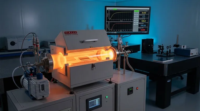
Achieve precise and repeatable thin film deposition with KINTEK.
Understanding the complex interplay of variables that determine your deposition rate is crucial for producing high-quality, consistent films. Whether you are working with PVD, CVD, or another technique, KINTEK provides the advanced lab equipment, consumables, and expert support you need to master your process.
We offer:
- State-of-the-art deposition systems with integrated in-situ monitoring capabilities.
- High-purity target materials and precursors for reliable performance.
- Technical expertise to help you model, control, and optimize your deposition parameters.
Ready to optimize your thin film process? Contact our experts today to discuss your specific laboratory requirements and discover how KINTEK's solutions can enhance your research and production outcomes.
Visual Guide
