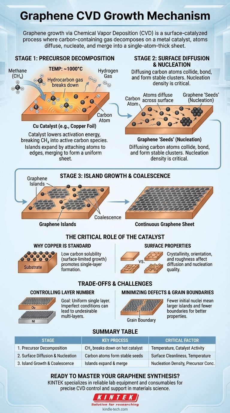
In short, the growth of graphene via Chemical Vapor Deposition (CVD) is a surface-catalyzed process. A carbon-containing gas, like methane, is introduced into a high-temperature chamber where it decomposes on a metal catalyst, typically copper. The resulting carbon atoms diffuse across the metal surface, nucleate into small graphene "islands," and then these islands grow and merge to form a continuous, single-atom-thick sheet.
At its core, CVD graphene growth is a delicate balance. You are choreographing the decomposition of a precursor gas and the self-assembly of carbon atoms on a catalyst surface, where precise control over temperature, pressure, and the catalyst itself determines the final quality of the film.
The Fundamental Stages of Graphene Growth
Understanding the CVD process requires breaking it down into three distinct, sequential stages. Each stage is a control point that directly influences the characteristics of the final graphene film.
Stage 1: Precursor Decomposition
The process begins by feeding a hydrocarbon gas (the precursor) into a reactor heated to around 1000 °C. Methane (CH₄) is a common choice.
At this high temperature, the metal substrate, most often a copper foil, acts as a catalyst. It lowers the energy required to break the chemical bonds in the precursor gas, causing it to decompose into active carbon species (radicals) on the metal's surface.
Stage 2: Surface Diffusion and Nucleation
Once freed, these individual carbon atoms are not static. They possess enough thermal energy to diffuse or "skate" across the hot catalyst surface.
Eventually, diffusing carbon atoms collide and bond, forming stable, small clusters. This initial formation of a graphene "seed" is called nucleation. The density of these nucleation sites is a critical parameter; too many sites lead to a film with many grain boundaries.
Stage 3: Island Growth and Coalescence
Each nucleation site acts as a seed for a growing graphene island. Carbon atoms diffusing on the surface preferentially attach to the open edges of these existing islands, causing them to expand outwards.
This growth continues until the individual islands meet and stitch together, a process known as coalescence. When properly controlled, this forms a continuous, uniform, single-layer graphene sheet covering the entire catalyst surface.
The Critical Role of the Catalyst
The choice of metal substrate is arguably the most important factor in the entire CVD process. It is not merely a surface to grow on; it is an active participant in the reaction.
Why Copper is the Standard
Copper is the most common catalyst for producing high-quality, single-layer graphene. This is due to its very low carbon solubility.
Because carbon does not dissolve well into bulk copper, the growth is "surface-limited." Carbon atoms remain on the surface, promoting the lateral growth of a single layer rather than precipitating multiple layers.
The Impact of Surface Properties
The quality of the catalyst surface itself is paramount. Factors like crystallinity, crystal facet orientation, and even microscopic surface roughness can dramatically affect how carbon atoms diffuse and where they nucleate.
A smooth, clean, and uniform catalyst surface is essential for minimizing defects and achieving large, single-crystal graphene domains.
Understanding the Trade-offs and Challenges
While the CVD process is powerful, achieving perfect graphene films is challenging. Control is a constant battle against competing physical phenomena.
Controlling Layer Number
The primary goal is often a uniform single layer. However, if conditions are not optimal (e.g., precursor flow is too high or cooling is too fast on a different catalyst like nickel), carbon can form multiple, stacked graphene layers in undesirable patches. This is a common failure mode.
Minimizing Defects and Grain Boundaries
When the separate graphene islands coalesce, the lines where they meet are called grain boundaries. These are structural imperfections that can degrade the electrical and mechanical properties of the graphene sheet.
Controlling the density of the initial nucleation sites is the key to minimizing these boundaries. Fewer nucleation sites mean larger individual islands and, consequently, a final film with fewer grain boundaries.
Making the Right Choice for Your Goal
Optimizing a CVD process requires aligning your parameters with a specific objective. The ideal conditions for one goal may be detrimental to another.
- If your primary focus is large-area, single-layer coverage: Use a copper catalyst and aim for a "diffusion-limited" regime with a low concentration of carbon precursor to promote large island growth and minimize nucleation density.
- If your primary focus is fundamental growth studies: Experiment with variations in precursor flux, temperature, and pressure to map out how these changes affect nucleation density and island shape.
- If your primary focus is device fabrication: Prioritize minimizing grain boundaries and wrinkles, as these defects scatter charge carriers and reduce device performance. This means investing in high-quality, pre-treated catalyst substrates.
Ultimately, mastering graphene CVD is about understanding and controlling the journey of a single carbon atom from a gas molecule to its final place in a crystalline lattice.
Summary Table:
| Stage | Key Process | Critical Factor |
|---|---|---|
| 1. Precursor Decomposition | Hydrocarbon gas (e.g., methane) breaks down on hot catalyst surface. | Temperature, Catalyst Activity |
| 2. Surface Diffusion & Nucleation | Carbon atoms diffuse and form stable graphene 'seeds'. | Surface Cleanliness, Temperature |
| 3. Island Growth & Coalescence | Islands expand and merge into a continuous graphene sheet. | Nucleation Density, Precursor Concentration |
Ready to Master Your Graphene Synthesis?
Understanding the growth mechanism is the first step. Achieving consistent, high-quality graphene requires precise control over the CVD process and the right equipment.
KINTEK specializes in lab equipment and consumables, serving the exact needs of researchers and engineers in materials science. We provide the reliable tools and expert support to help you optimize your parameters, minimize defects, and push the boundaries of your graphene applications.
Contact our experts today to discuss how we can support your lab's innovation in 2D materials.
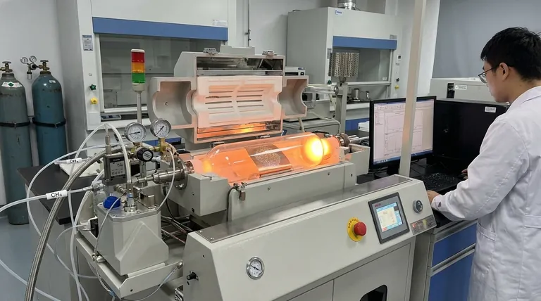
Visual Guide
Related Products
- Microwave Plasma Chemical Vapor Deposition MPCVD Machine System Reactor for Lab and Diamond Growth
- Cylindrical Resonator MPCVD Machine System Reactor for Microwave Plasma Chemical Vapor Deposition and Lab Diamond Growth
- 915MHz MPCVD Diamond Machine Microwave Plasma Chemical Vapor Deposition System Reactor
- Chemical Vapor Deposition CVD Equipment System Chamber Slide PECVD Tube Furnace with Liquid Gasifier PECVD Machine
- Customer Made Versatile CVD Tube Furnace Chemical Vapor Deposition Chamber System Equipment
People Also Ask
- How is a diamond formed from CVD? The Science of Growing Diamonds Atom by Atom
- How does MPCVD work? A Guide to Low-Temperature, High-Quality Film Deposition
- Why is argon-rich gas phase chemistry used for UNCD growth? Unlock Precision Nano-Diamond Synthesis
- How are CVD diamonds created? Discover the Science of Lab-Grown Diamond Precision
- What are the advantages of a Microwave Plasma CVD reactor for MCD/NCD coatings? Precision Multilayer Diamond Engineering


