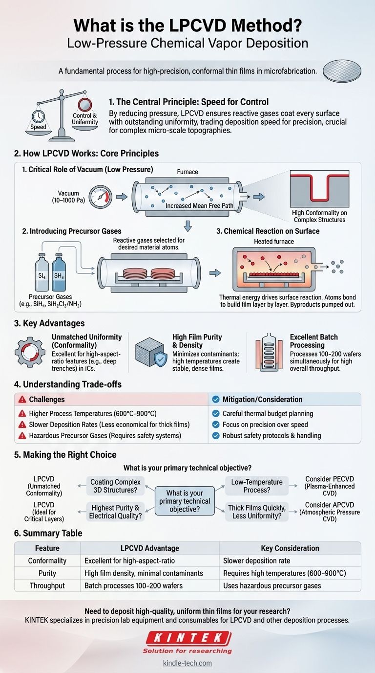
In short, LPCVD stands for Low-Pressure Chemical Vapor Deposition. It is a fundamental process in microfabrication used to deposit exceptionally uniform and pure thin films onto a substrate, typically a silicon wafer. By operating in a vacuum, LPCVD overcomes the limitations of atmospheric pressure methods, allowing it to coat highly complex, three-dimensional structures with precision, which is critical for modern semiconductor devices.
The central principle of LPCVD is trading speed for control. By significantly reducing the pressure, the process ensures that reactive gases coat every surface of a substrate with outstanding uniformity, making it the go-to method for creating high-quality, conformal films on complex micro-scale topographies.
How LPCVD Works: The Core Principles
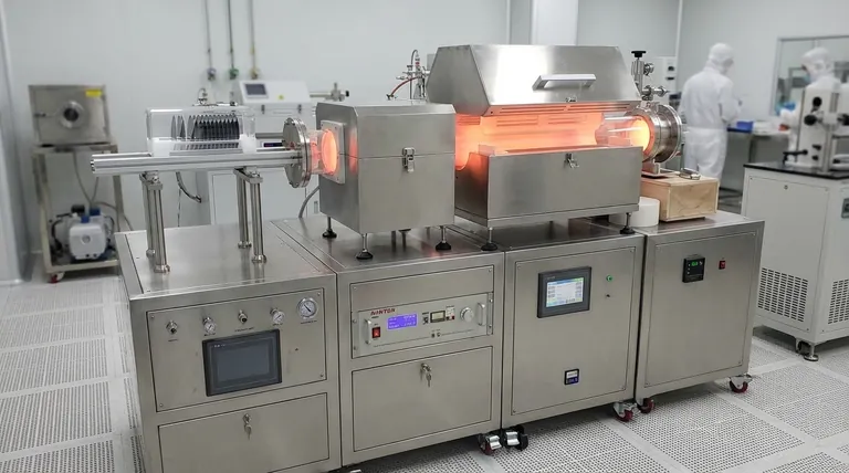
To understand why LPCVD is so effective, we must look at how its core components—low pressure, precursor gases, and thermal energy—work together. The process takes place inside a sealed furnace tube that is heated to a precise temperature.
The Critical Role of Vacuum (Low Pressure)
The "Low-Pressure" aspect is the key differentiator. The process chamber is pumped down to a vacuum (typically 10-1000 Pa), which is much lower than atmospheric pressure.
This vacuum dramatically increases the mean free path of the gas molecules—the average distance a molecule travels before colliding with another. In a nearly empty chamber, gas molecules are more likely to collide with the wafer surface than with each other, ensuring they arrive from all possible angles.
This leads to the single greatest advantage of LPCVD: high conformality. The film deposits evenly over flat surfaces, down deep trenches, and around sharp corners.
Introducing the Precursor Gases
Once the chamber is at the correct temperature and pressure, one or more reactive gases, known as precursors, are introduced. These gases are carefully selected to contain the atoms of the material you wish to deposit.
For example, to deposit a film of polysilicon, the precursor gas might be silane (SiH₄). For silicon nitride, a common insulating material, a mix of dichlorosilane (SiH₂Cl₂) and ammonia (NH₃) is often used.
The Chemical Reaction on the Surface
The heated wafers provide the thermal energy needed to drive a chemical reaction. When the precursor gas molecules strike the hot substrate surface, they decompose or react.
The desired atoms bond to the surface, building the thin film layer by layer. The other atoms from the precursor form volatile byproducts that are then pumped out of the chamber. Because this process is limited by the rate of the surface reaction rather than gas transport, deposition is slow but extremely uniform across the wafer.
Why Choose LPCVD? Key Advantages
LPCVD is not the only deposition method, but its unique characteristics make it indispensable for specific, high-value applications.
Unmatched Film Uniformity (Conformality)
As mentioned, the long mean free path of gas molecules allows LPCVD to produce films with excellent conformality. This is non-negotiable for manufacturing modern integrated circuits, where features have high aspect ratios (they are much deeper than they are wide).
High Film Purity and Density
Operating in a vacuum minimizes the risk of incorporating atmospheric contaminants like oxygen or water vapor into the growing film. The high process temperatures also result in dense, stable films with excellent electrical and mechanical properties.
Excellent Batch Processing Capability
Because the process is not limited by gas flow dynamics, wafers can be stacked vertically in a quartz carrier, or "boat." This allows a single LPCVD furnace to process 100-200 wafers simultaneously, achieving high overall throughput despite the relatively slow deposition rate per wafer.
Understanding the Trade-offs
No process is perfect. LPCVD's advantages come with specific limitations that must be considered.
Higher Process Temperatures
LPCVD typically requires high temperatures (600°C to over 900°C) to drive the necessary surface reactions. This high thermal budget can be a problem for devices that have already undergone fabrication steps with materials that cannot withstand such heat, such as aluminum interconnects.
Slower Deposition Rates
Compared to atmospheric pressure methods (APCVD), LPCVD is significantly slower. This makes it less economical for applications where a very thick film is needed and perfect uniformity is not the primary concern.
Hazardous Precursor Gases
Many of the precursor gases used in LPCVD are highly toxic, flammable, or pyrophoric (igniting spontaneously in air). This necessitates sophisticated safety systems, gas monitoring, and handling protocols, adding to the cost and complexity of the operation.
Making the Right Choice for Your Goal
Selecting a deposition method requires a clear understanding of your primary technical objective. LPCVD is a powerful tool, but only when applied to the right problem.
- If your primary focus is coating complex 3D structures: LPCVD is the superior choice due to its unmatched conformality.
- If your primary focus is the highest possible film purity and electrical quality: LPCVD is ideal for critical layers like gate polysilicon or high-quality nitride dielectrics.
- If your primary focus is a low-temperature process: LPCVD is likely unsuitable; consider Plasma-Enhanced CVD (PECVD), which uses plasma energy to allow deposition at lower temperatures.
- If your primary focus is depositing thick films quickly with less concern for uniformity: Atmospheric Pressure CVD (APCVD) is a more economical and faster alternative.
Understanding these trade-offs empowers you to select the precise deposition tool required to achieve your device performance and manufacturing goals.
Summary Table:
| Feature | LPCVD Advantage | Key Consideration |
|---|---|---|
| Conformality | Excellent for high-aspect-ratio structures | Slower deposition rate |
| Purity | High film density, minimal contaminants | Requires high temperatures (600–900°C) |
| Throughput | Batch processes 100-200 wafers simultaneously | Uses hazardous precursor gases |
Need to deposit high-quality, uniform thin films for your semiconductor or advanced materials research? KINTEK specializes in providing precision lab equipment and consumables for LPCVD and other deposition processes. Our solutions help you achieve the film purity and conformality critical for next-generation devices. Contact our experts today to discuss how we can support your laboratory's microfabrication needs.
Visual Guide
Related Products
- Chemical Vapor Deposition CVD Equipment System Chamber Slide PECVD Tube Furnace with Liquid Gasifier PECVD Machine
- Inclined Rotary Plasma Enhanced Chemical Vapor Deposition PECVD Equipment Tube Furnace Machine
- RF PECVD System Radio Frequency Plasma-Enhanced Chemical Vapor Deposition RF PECVD
- Microwave Plasma Chemical Vapor Deposition MPCVD Machine System Reactor for Lab and Diamond Growth
- 915MHz MPCVD Diamond Machine Microwave Plasma Chemical Vapor Deposition System Reactor
People Also Ask
- How expensive is chemical vapor deposition? Understanding the True Cost of High-Performance Coating
- What types of substrates are used in CVD to facilitate graphene films? Optimize Graphene Growth with the Right Catalyst
- What are the core advantages of PE-CVD in OLED encapsulation? Protect Sensitive Layers with Low-Temp Film Deposition
- What are the processes of vapor phase deposition? Understand CVD vs. PVD for Superior Thin Films
- What is the chemical vapor deposition growth process? Build Superior Thin Films from the Atom Up


