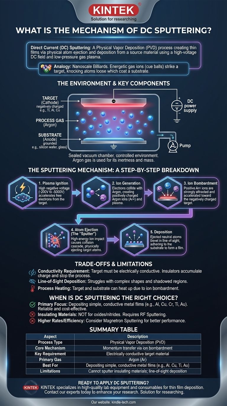
Direct Current (DC) sputtering is a physical vapor deposition (PVD) process that creates a thin film by physically ejecting atoms from a source material and depositing them onto a substrate. It works by establishing a high-voltage DC electric field within a low-pressure gas environment. This field creates a plasma, and the positively charged ions from this plasma are accelerated to bombard the source material, dislodging atoms that then coat the substrate.
At its core, DC sputtering is a momentum transfer process, not a chemical or thermal one. Think of it as a nanoscale game of billiards: energetic gas ions act as cue balls, striking a target of source material and knocking atoms loose, which then travel and stick to a nearby substrate.
The Environment and Key Components
Before the process can begin, the system's components must be correctly configured within a controlled environment. This setup is fundamental to the entire mechanism.
The Vacuum Chamber
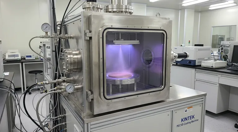
The entire process occurs inside a sealed vacuum chamber. This is critical for two reasons: it removes atmospheric gases that could contaminate the film, and it allows the sputtered atoms to travel freely from the target to the substrate with minimal collisions.
The Target (Cathode)
The target is a solid block of the material you wish to deposit (e.g., titanium, aluminum, copper). It is connected to the negative terminal of a DC power supply, making it the cathode.
The Substrate (Anode)
This is the object you want to coat, such as a silicon wafer, a piece of glass, or a medical implant. It is typically placed facing the target and is often at ground potential, effectively making it the anode.
The Process Gas (Argon)
After creating a vacuum, the chamber is backfilled with a small, controlled amount of an inert gas, most commonly Argon (Ar). Argon is used because it is chemically inert, has sufficient mass to eject target atoms effectively, and is relatively inexpensive.
The Sputtering Mechanism: A Step-by-Step Breakdown
Once the environment is established, the DC voltage is applied, initiating a precise chain of events that leads to film formation.
Step 1: Plasma Ignition
A strong negative voltage (typically -200V to -5000V) is applied to the target. This high voltage pulls stray free electrons and accelerates them away from the target at high speed.
Step 2: Ion Generation
As these energetic electrons travel through the chamber, they collide with neutral Argon gas atoms. If the electron has enough energy, it will knock an electron off the Argon atom, creating a positively charged Argon ion (Ar+) and another free electron. This process repeats, creating a self-sustaining cascade that results in a glowing, ionized gas known as a plasma.
Step 3: Ion Bombardment
The newly formed positive Argon ions (Ar+) are now strongly attracted and accelerated toward the negatively charged target. They strike the target's surface with significant kinetic energy.
Step 4: Atom Ejection (The "Sputter")
The impact of a high-energy ion does not melt or vaporize the target. Instead, it triggers a collision cascade within the target material, transferring its momentum to the target's atoms. When this cascade of energy reaches the surface, it can give a surface atom enough energy to overcome its atomic bonds and be physically ejected into the vacuum chamber. This ejected atom is the "sputtered" particle.
Step 5: Deposition
The sputtered neutral atoms travel in a straight line, or "line of sight," through the low-pressure chamber. When they strike the substrate, they stick to its surface (adsorption) and begin to build up, layer by layer, to form a dense and uniform thin film.
Understanding the Trade-offs and Limitations
While powerful, the DC sputtering mechanism has inherent limitations that are critical to understand.
The Conductivity Requirement
The most significant limitation of DC sputtering is that the target material must be electrically conductive. A non-conductive (insulating) target would quickly accumulate a positive charge from the bombarding ions, neutralizing the electric field and shutting down the sputtering process.
Line-of-Sight Deposition
Because sputtered atoms travel in straight lines, the process can struggle to uniformly coat complex, three-dimensional shapes with shadowed regions or undercuts. This can result in a thinner or non-existent film on certain surfaces.
Process Heating
The constant bombardment of energetic ions transfers a significant amount of heat to the target. This energy can also radiate and heat the substrate, which may be undesirable when coating temperature-sensitive materials like plastics.
When is DC Sputtering the Right Choice?
Choosing a deposition technique requires matching the process capabilities to your end goal. DC sputtering is a foundational method with a clear-cut application space.
- If your primary focus is depositing a simple, conductive metal film: DC sputtering is an extremely reliable, well-understood, and cost-effective choice for materials like aluminum, copper, chromium, titanium, and gold.
- If you need to deposit an insulating or dielectric material (like an oxide or nitride): You must use an alternative technique like RF (Radio Frequency) Sputtering, which uses an AC field to avoid charge buildup on the target.
- If you require higher deposition rates and more efficient use of your target material: You should investigate Magnetron Sputtering, a common enhancement that uses magnets to trap electrons near the target, dramatically increasing ionization efficiency.
Understanding this fundamental mechanism of physical momentum transfer is the key to selecting the right deposition technique for your specific material and application goals.
Summary Table:
| Aspect | Description |
|---|---|
| Process Type | Physical Vapor Deposition (PVD) |
| Core Mechanism | Momentum transfer via ion bombardment |
| Key Requirement | Electrically conductive target material |
| Primary Gas | Argon (Ar) |
| Best For | Depositing simple, conductive metal films (e.g., Al, Cu, Ti, Au) |
| Limitations | Cannot sputter insulating materials; line-of-sight deposition |
Ready to apply DC sputtering in your lab?
KINTEK specializes in high-quality lab equipment and consumables for all your thin film deposition needs. Whether you are researching new materials or scaling up production, our expertise ensures you have the right tools for precise and reliable results.
Contact our experts today to discuss how our sputtering solutions can enhance your laboratory's capabilities and drive your projects forward.
Visual Guide
Related Products
- Laboratory Scientific Electric Heating Blast Drying Oven
- Single Punch Electric Tablet Press Machine TDP Tablet Punching Machine
People Also Ask
- What is the necessity of using a laboratory drying oven when processing MoO3/GO composite nanopowders? Find out here.
- What is the role of a laboratory blast drying oven in the production of solid-state corrosion inhibitors? - KINTEK
- What is the function of a laboratory drying oven in Zr2.5Nb alloy pretreatment? Ensure Precise Corrosion Test Results
- What role does a precision laboratory drying oven play in the synthesis of GO-PANI nanocomposites? Protect Material Integrity
- What is the role of a laboratory drying oven in cellulose citrate production? Ensure Material Stability & Purity

