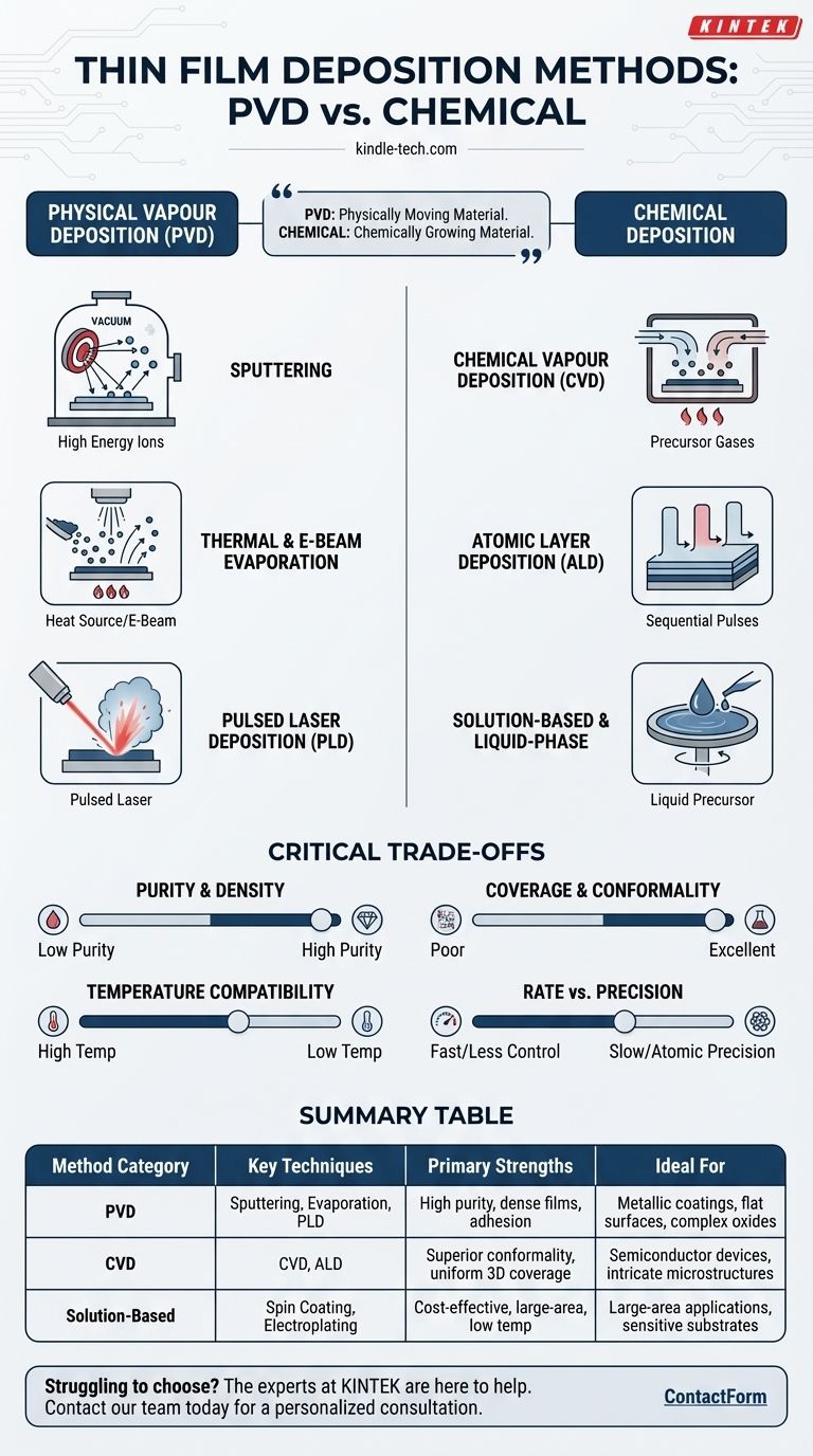
The primary methods for depositing thin films are broadly categorized into two families: Physical Vapour Deposition (PVD) and Chemical Deposition. PVD involves physically transferring a material from a source to a substrate, typically in a vacuum, using techniques like sputtering or evaporation. Chemical methods, such as Chemical Vapour Deposition (CVD), use chemical reactions from precursor gases to form a solid film on the substrate's surface.
The core distinction between deposition methods is not just technique, but philosophy. Your choice depends on a fundamental trade-off: are you physically moving solid material onto a surface (PVD), or are you chemically growing a new material directly on that surface (CVD)? This decision dictates the film's purity, structure, and ability to coat complex shapes.
The Two Pillars of Deposition: Physical vs. Chemical
At the highest level, all thin film deposition techniques fall into one of two categories. Understanding this distinction is the first step in selecting the correct process for an application.
The Physical Approach
Physical methods involve the atom-by-atom or molecule-by-molecule transfer of a material from a source to a substrate. These processes are almost always conducted in a vacuum to ensure the transferred particles travel without colliding with air molecules.
The Chemical Approach
Chemical methods create the film through chemical reactions that occur directly on the substrate surface. These methods can range from high-vacuum processes using reactive gases to simpler liquid-phase techniques like electroplating or spin coating.
Exploring Physical Vapour Deposition (PVD)
PVD is a "line-of-sight" process, meaning the source material must have an unobstructed path to the substrate. It is renowned for creating high-purity, dense films.
Sputtering
In sputtering, a solid target of the desired material is bombarded with high-energy ions (usually an inert gas like Argon). This bombardment physically ejects, or "sputters," atoms from the target, which then travel and deposit onto the substrate.
This method is highly versatile and can be used to deposit metals, alloys, and compounds with excellent adhesion.
Thermal & E-Beam Evaporation
This is one of the simplest PVD concepts. The source material is heated in a high vacuum until it evaporates. These vaporized atoms then travel through the vacuum and condense on the cooler substrate, forming a thin film.
Electron beam (e-beam) evaporation is a more precise version where a high-energy electron beam is used to heat the source material, offering better control over the deposition rate.
Pulsed Laser Deposition (PLD)
In PLD, a high-power pulsed laser is focused on a target in a vacuum. The intense energy ablates material from the target, creating a plasma plume that expands and deposits onto the substrate. This is particularly useful for depositing complex materials like oxides.
Exploring Chemical Deposition Methods
Chemical deposition methods are not limited by line-of-sight, giving them a key advantage in coating complex, three-dimensional structures with a uniform film.
Chemical Vapour Deposition (CVD)
CVD is a workhorse in the semiconductor industry. It involves introducing one or more volatile precursor gases into a reaction chamber. These gases react or decompose on a heated substrate to produce the desired solid film.
Because the deposition depends on a chemical reaction on the surface, CVD provides excellent conformal coverage over intricate topographies.
Atomic Layer Deposition (ALD)
ALD is a specialized, highly controlled subtype of CVD. It builds the film literally one atomic layer at a time by introducing precursor gases in sequential, self-limiting pulses.
While much slower than other methods, ALD offers unparalleled precision in thickness control and perfect conformality, which is critical for modern microelectronics.
Solution-Based & Liquid-Phase Methods
Simpler chemical methods are performed without high vacuum. Techniques like spin coating, sol-gel, dip coating, and electroplating use a liquid precursor to deposit a film. These are often lower-cost and suitable for large-area applications where ultimate purity or density is not the primary concern.
Understanding the Critical Trade-offs
No single deposition method is universally superior. The choice always involves balancing competing factors based on the final application's requirements.
Purity and Density
PVD methods, especially sputtering and e-beam evaporation, generally produce films with higher purity and density. The vacuum environment minimizes contamination, and the energetic nature of the deposition creates a tightly packed film structure.
Coverage and Conformality
This is the primary advantage of chemical methods. CVD and especially ALD excel at coating deep trenches and complex 3D shapes uniformly, whereas line-of-sight PVD would leave "shadowed" areas uncoated.
Temperature and Substrate Compatibility
Many CVD processes require very high substrate temperatures to drive the necessary chemical reactions. This can damage sensitive substrates like plastics or certain electronic components. Sputtering, in contrast, can often be performed at much lower temperatures.
Rate vs. Precision
There is a direct trade-off between deposition speed and control. Thermal evaporation can be very fast but offers less control over film structure. At the other extreme, ALD offers atomic-level precision but is exceptionally slow.
Making the Right Choice for Your Goal
Selecting the correct method requires aligning the technique's strengths with your primary objective.
- If your primary focus is high-purity, dense metallic coatings on a flat surface: PVD techniques like sputtering or e-beam evaporation are the industry standard.
- If your primary focus is uniform coverage over complex 3D microstructures: CVD is the most effective choice, with ALD providing the ultimate in precision and conformality.
- If your primary focus is depositing complex oxide materials with specific stoichiometry: Pulsed Laser Deposition (PLD) or reactive sputtering are often the best options.
- If your primary focus is cost-effective, large-area coating without high-vacuum requirements: Solution-based methods like spin coating or spray pyrolysis should be considered.
Understanding the fundamental principles of physical and chemical deposition empowers you to select the precise tool required to engineer materials at the atomic scale.
Summary Table:
| Method Category | Key Techniques | Primary Strengths | Ideal For |
|---|---|---|---|
| Physical Vapour Deposition (PVD) | Sputtering, Evaporation, PLD | High purity, dense films, excellent adhesion | Metallic coatings, flat surfaces, complex oxides |
| Chemical Vapour Deposition (CVD) | CVD, ALD | Superior conformality, uniform 3D coverage | Semiconductor devices, intricate microstructures |
| Solution-Based Methods | Spin Coating, Electroplating | Cost-effective, large-area coating, low temperature | Large-area applications, sensitive substrates |
Struggling to choose the right thin film deposition method for your specific application? The experts at KINTEK are here to help. We specialize in providing the ideal lab equipment and consumables for both PVD and CVD processes, ensuring you achieve the precise film properties—whether it's high purity, perfect conformality, or cost-effective large-area coating—that your research or production demands.
Let us help you optimize your thin film deposition process. Contact our team today for a personalized consultation and discover how KINTEK's solutions can enhance your laboratory's capabilities.
Visual Guide
Related Products
- Aluminized Ceramic Evaporation Boat for Thin Film Deposition
- Tungsten Evaporation Boat for Thin Film Deposition
- Electron Beam Evaporation Coating Oxygen-Free Copper Crucible and Evaporation Boat
- Molybdenum Tungsten Tantalum Evaporation Boat for High Temperature Applications
- Vacuum Hot Press Furnace Machine for Lamination and Heating
People Also Ask
- Why is an alumina boat and Ti3AlC2 powder bed necessary for Ti2AlC sintering? Protect MAX Phase Purity
- What are the applications of thin films deposition? Unlock New Possibilities for Your Materials
- What are the alternatives to sputtering? Choose the Right Thin Film Deposition Method
- What is the chemical method for thin film deposition? Build Films from the Molecular Level Up
- Why are high-purity ceramic boats used for lignin activation? Ensure Purity & Thermal Stability


