At its core, Physical Vapor Deposition (PVD) is a family of vacuum-based coating techniques where a solid material is converted into a vapor, transported across a chamber, and condensed onto a target surface (the substrate) to form a high-performance thin film. This atom-by-atom deposition process allows for extremely precise control over the film's thickness, structure, and properties.
PVD is not a chemical reaction. It is a purely physical process of changing a material's state—from solid to vapor and back to a solid thin film—making it a versatile tool for enhancing the surface properties of an object without altering the material's fundamental chemistry.
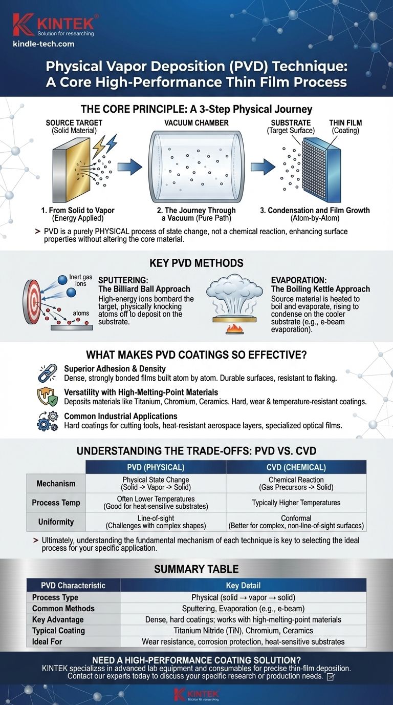
The Core Principle: A Physical Transformation
Understanding PVD is to understand a three-step physical journey that takes place inside a vacuum. This process is what gives PVD coatings their unique and valuable characteristics.
From Solid to Vapor
The process begins with a solid source material, often called the target. Energy is applied to this target to liberate atoms or molecules and convert them into a vapor. How this energy is applied defines the specific P-V-D method.
The Journey Through a Vacuum
This vapor travels through a low-pressure vacuum chamber. The vacuum is critical because it removes other atoms and molecules (like air) that could collide with and contaminate the depositing material, ensuring a pure film.
Condensation and Film Growth
When the vapor particles reach the cooler substrate (the object being coated), they condense back into a solid state. This happens atom-by-atom, building up a thin, dense, and highly adherent film on the substrate's surface.
Key PVD Methods Explained
While the principle is the same, the method of vaporizing the target material varies. The two most common approaches represent different ways of applying energy.
Sputtering: The Billiard Ball Approach
In sputtering, the target is bombarded with high-energy ions (typically of an inert gas like Argon). These ions act like microscopic billiard balls, physically knocking atoms off the target material. These "sputtered" atoms then travel to and deposit on the substrate.
Evaporation: The Boiling Kettle Approach
In thermal evaporation, the source material is heated in the vacuum chamber until it begins to boil and evaporate, much like water in a kettle. This vapor then rises, travels to the substrate, and condenses to form the coating. A common technique is e-beam evaporation, which uses a focused electron beam to heat the material.
What Makes PVD Coatings So Effective?
PVD is used across industries because the resulting films offer significant performance enhancements.
Superior Adhesion and Density
Because the film is built atom by atom in a controlled environment, PVD coatings are typically very dense and strongly bonded to the substrate. This results in durable surfaces that resist flaking or chipping.
Versatility with High-Melting-Point Materials
PVD can effectively deposit materials with extremely high melting points, such as titanium, chromium, and various ceramics. This makes it ideal for creating hard, wear-resistant, and temperature-resistant coatings that would be difficult to apply otherwise.
Common Industrial Applications
The properties of PVD coatings make them invaluable in many fields. They are used to apply hard, corrosion-resistant coatings on cutting tools, dense, heat-resistant layers on aerospace components, and specialized optical films for semiconductors and solar panels.
Understanding the Trade-offs: PVD vs. CVD
To fully grasp PVD, it's helpful to contrast it with its counterpart, Chemical Vapor Deposition (CVD). While both create thin films, their mechanisms are fundamentally different.
The Fundamental Difference: Physical vs. Chemical
PVD is a physical process; the coating material is the same as the source material, just in a different form. Chemical Vapor Deposition (CVD), by contrast, is a chemical process where precursor gases react on the substrate's surface to form an entirely new solid material as the coating.
Process Temperature and Substrate Impact
PVD processes can often be conducted at lower temperatures than many traditional CVD processes. This makes PVD suitable for coating heat-sensitive materials, such as plastics or certain metal alloys, that could be damaged by high-temperature chemical reactions.
Coating Uniformity and Geometry
Because PVD is typically a "line-of-sight" process (atoms travel in a straight line from target to substrate), it can be challenging to evenly coat complex, three-dimensional shapes. CVD, which uses a gas that can flow around an object, is often better at creating uniform (conformal) coatings on intricate surfaces.
Making the Right Choice for Your Goal
Selecting the right deposition method requires understanding your end goal. The choice between PVD and CVD, or even between different PVD methods, depends entirely on the desired outcome for your component.
- If your primary focus is durability and wear-resistance: PVD is an exceptional choice for applying very hard, dense coatings like Titanium Nitride (TiN) to tools and industrial components.
- If your primary focus is coating heat-sensitive materials: PVD's typically lower process temperatures give it an advantage for substrates that cannot withstand the heat of many CVD processes.
- If your primary focus is a chemically unique film or coating complex 3D shapes: Chemical Vapor Deposition (CVD) may be more suitable due to its reactive nature and ability to uniformly coat non-line-of-sight surfaces.
Ultimately, understanding the fundamental mechanism of each technique is the key to selecting the ideal process for your specific application.
Summary Table:
| PVD Characteristic | Key Detail |
|---|---|
| Process Type | Physical (solid → vapor → solid) |
| Common Methods | Sputtering, Evaporation (e.g., e-beam) |
| Key Advantage | Dense, hard coatings; works with high-melting-point materials |
| Typical Coating | Titanium Nitride (TiN), Chromium, Ceramics |
| Ideal For | Wear resistance, corrosion protection, heat-sensitive substrates |
Need a high-performance coating solution for your laboratory components? The right PVD process can dramatically enhance the durability and functionality of your tools and parts. KINTEK specializes in providing advanced lab equipment and consumables for precise thin-film deposition. Contact our experts today to discuss how our PVD solutions can meet your specific research or production needs and bring superior performance to your lab.
Visual Guide
Related Products
- Chemical Vapor Deposition CVD Equipment System Chamber Slide PECVD Tube Furnace with Liquid Gasifier PECVD Machine
- RF PECVD System Radio Frequency Plasma-Enhanced Chemical Vapor Deposition RF PECVD
- 915MHz MPCVD Diamond Machine Microwave Plasma Chemical Vapor Deposition System Reactor
- HFCVD Machine System Equipment for Drawing Die Nano-Diamond Coating
- Microwave Plasma Chemical Vapor Deposition MPCVD Machine System Reactor for Lab and Diamond Growth
People Also Ask
- How are carbon nanotubes grown? Master Scalable Production with Chemical Vapor Deposition
- What is plasma enhanced chemical vapor deposition PECVD equipment? A Guide to Low-Temperature Thin Film Deposition
- How expensive is chemical vapor deposition? Understanding the True Cost of High-Performance Coating
- What types of substrates are used in CVD to facilitate graphene films? Optimize Graphene Growth with the Right Catalyst
- What is the chemical vapor deposition growth process? Build Superior Thin Films from the Atom Up


