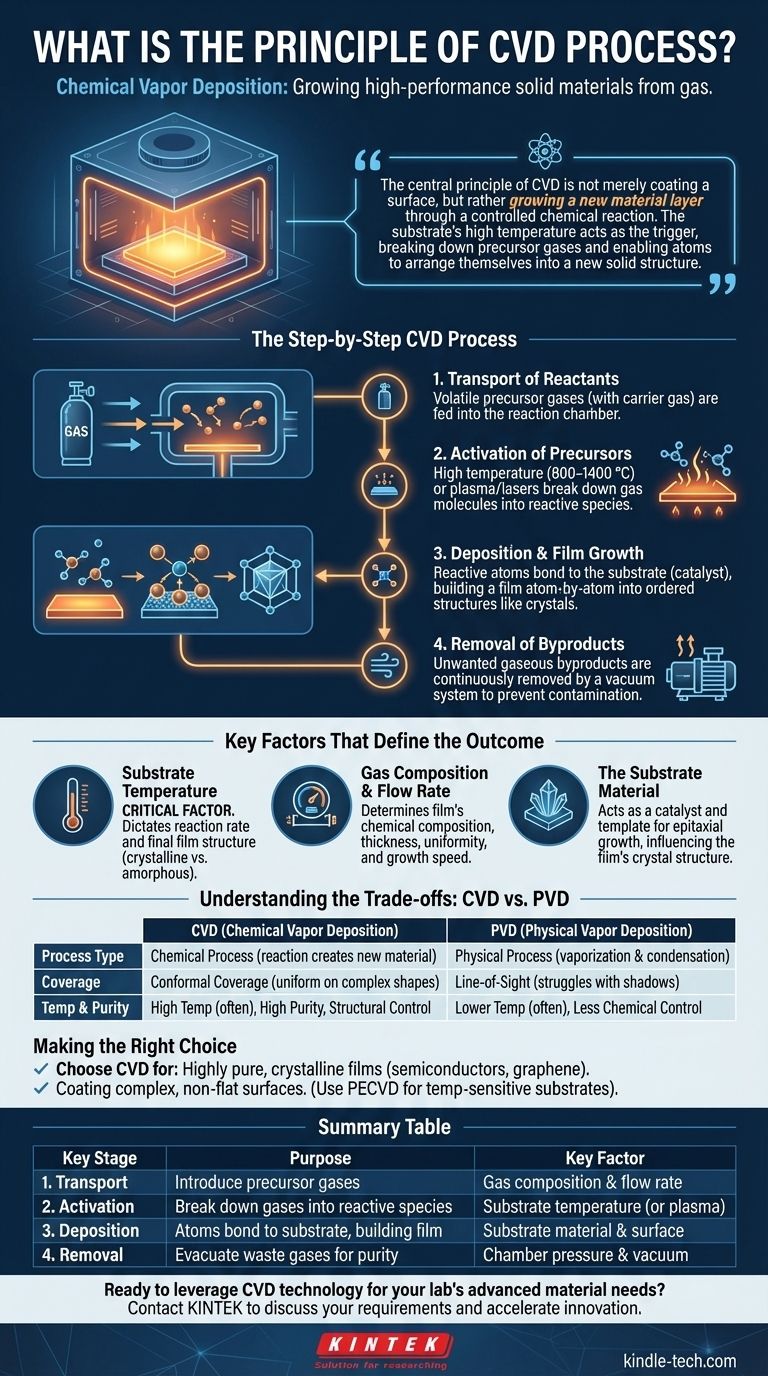
At its core, Chemical Vapor Deposition (CVD) is a process for manufacturing high-performance solid materials from a gas. It works by introducing specific precursor gases into a reaction chamber containing a heated object, known as a substrate. The heat provides the energy for a chemical reaction to occur on the substrate’s surface, resulting in the growth of a thin, solid film with precisely controlled properties.
The central principle of CVD is not merely coating a surface, but rather growing a new material layer through a controlled chemical reaction. The substrate's high temperature acts as the trigger, breaking down precursor gases and enabling atoms to arrange themselves into a new solid structure.
The Step-by-Step CVD Process
To truly grasp the principle of CVD, it's best to break it down into its fundamental stages. Each step is carefully controlled to achieve the desired film thickness, composition, and structure.
1. Transport of Reactants
The process begins by feeding one or more volatile precursor gases into a controlled reaction chamber. These gases contain the atoms that will form the final film.
Often, these precursors are diluted with an inert carrier gas (like argon or nitrogen) to manage their concentration and ensure a stable, uniform flow over the substrate.
2. Activation of Precursors
For a reaction to occur, the stable precursor gas molecules must be broken down into more reactive species. This activation is typically achieved by heating the substrate to very high temperatures, often between 800 °C and 1400 °C.
When gas molecules contact the hot surface, they gain enough thermal energy to dissociate, or break their chemical bonds. In some advanced CVD methods, this energy can be supplied by a plasma (PECVD) or lasers instead of just heat.
3. Deposition and Film Growth
The highly reactive atoms and molecules now diffuse across the substrate's surface. They find stable locations and undergo chemical reactions, bonding with the surface and with each other.
This is an atomistic process, where the film is built up atom by atom or molecule by molecule. The substrate itself often acts as a catalyst, promoting the reaction and ensuring the new film adheres strongly to its surface. This controlled growth allows for the formation of highly ordered crystalline films, like synthetic diamond or graphene.
4. Removal of Byproducts
The chemical reactions that form the solid film also create unwanted gaseous byproducts. These waste gases are continuously removed from the reaction chamber by a vacuum system to prevent them from contaminating the film or interfering with the deposition process.
Key Factors That Define the Outcome
The success of the CVD process hinges on the precise control of several key variables. Changing any one of these can dramatically alter the properties of the final material.
Substrate Temperature
This is arguably the most critical factor. The temperature dictates the rate of the chemical reaction and influences the final structure of the film (e.g., crystalline vs. amorphous).
Gas Composition and Flow Rate
The specific precursor gases used determine the chemical composition of the film. The flow rate and pressure inside the chamber affect the film's thickness, uniformity, and growth speed.
The Substrate Material
The substrate is not just a passive holder. Its surface can catalyze the reaction, and its own crystal structure can serve as a template for the growing film, a process known as epitaxial growth.
Understanding the Trade-offs: CVD vs. PVD
To fully appreciate CVD, it is helpful to contrast it with its main alternative, Physical Vapor Deposition (PVD).
Chemical Reaction vs. Physical Deposition
The defining difference is in the name. CVD is a chemical process, creating a new material on the substrate. PVD is a physical process, where a solid material is vaporized (e.g., by evaporation or sputtering) and then simply condenses on the substrate, with no chemical reaction occurring.
Conformal Coverage
Because CVD relies on a gas that can flow into and around any feature, it excels at producing a uniform, conformal coating on complex, three-dimensional shapes. PVD is typically a line-of-sight process and struggles to coat shadowed areas evenly.
Temperature and Complexity
Traditional CVD requires very high temperatures, which can damage sensitive substrates. PVD can often be performed at lower temperatures. However, the chemical nature of CVD allows for the creation of compounds and alloys with a level of purity and structural control that is difficult to achieve with physical methods.
Making the Right Choice for Your Goal
Understanding the core principle of CVD helps you determine when it is the most effective manufacturing technique for a specific application.
- If your primary focus is a highly pure, crystalline film: CVD is often the superior choice, as it chemically "grows" the material with precise control over its atomic structure, essential for materials like semiconductors, graphene, or diamonds.
- If your primary focus is coating a complex, non-flat surface: CVD's gas-based nature provides excellent conformal coverage that physical methods struggle to match, making it ideal for coating intricate components.
- If your primary focus is deposition on a temperature-sensitive material: You must consider a lower-temperature CVD variant like Plasma-Enhanced CVD (PECVD), which uses plasma instead of extreme heat to activate the precursors.
By controlling a chemical reaction at the atomic level, CVD transforms simple gases into some of the most advanced materials in modern technology.
Summary Table:
| Key Stage | Purpose | Key Factor |
|---|---|---|
| 1. Transport of Reactants | Introduce precursor gases into the chamber | Gas composition and flow rate |
| 2. Activation of Precursors | Break down gases into reactive species using heat/plasma | Substrate temperature |
| 3. Deposition & Film Growth | Atoms bond to the substrate, building the film layer-by-layer | Substrate material and surface properties |
| 4. Removal of Byproducts | Evacuate waste gases to ensure film purity | Chamber pressure and vacuum system |
Ready to leverage CVD technology for your lab's advanced material needs? KINTEK specializes in high-performance lab equipment and consumables, providing the precise control and reliability required for successful Chemical Vapor Deposition processes. Whether you are developing semiconductors, coatings, or graphene, our solutions are designed to help you grow superior materials. Contact our experts today to discuss how we can support your specific laboratory requirements and accelerate your innovation.
Visual Guide
Related Products
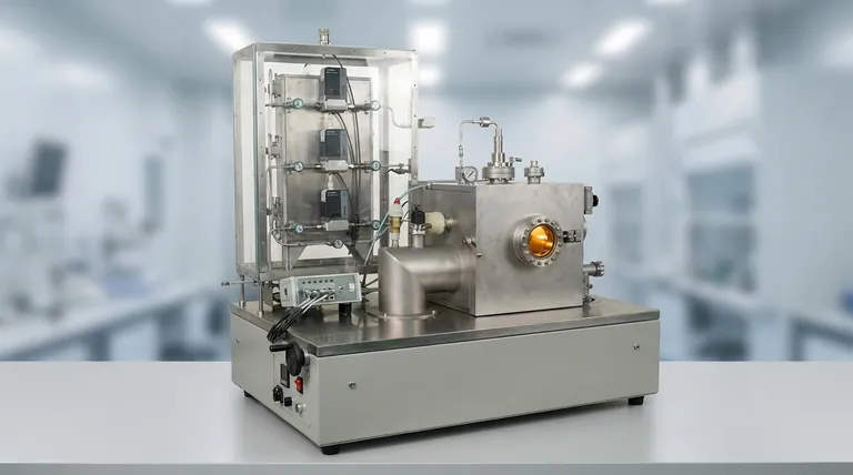
- Chemical Vapor Deposition CVD Equipment System Chamber Slide PECVD Tube Furnace with Liquid Gasifier PECVD Machine
- RF PECVD System Radio Frequency Plasma-Enhanced Chemical Vapor Deposition RF PECVD
- Microwave Plasma Chemical Vapor Deposition MPCVD Machine System Reactor for Lab and Diamond Growth
- Customer Made Versatile CVD Tube Furnace Chemical Vapor Deposition Chamber System Equipment
- 915MHz MPCVD Diamond Machine Microwave Plasma Chemical Vapor Deposition System Reactor
People Also Ask
- What are the processes of vapor phase deposition? Understand CVD vs. PVD for Superior Thin Films
- What is plasma enhanced chemical vapor deposition PECVD equipment? A Guide to Low-Temperature Thin Film Deposition
- How are carbon nanotubes grown? Master Scalable Production with Chemical Vapor Deposition
- What are the core advantages of PE-CVD in OLED encapsulation? Protect Sensitive Layers with Low-Temp Film Deposition
- Why is Chemical Vapor Deposition (CVD) equipment uniquely suited for constructing hierarchical superhydrophobic structures?


