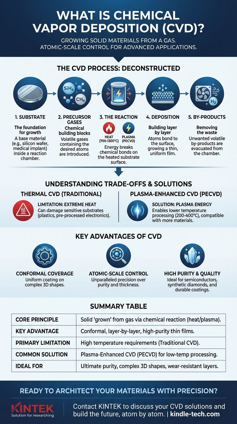
At its core, Chemical Vapor Deposition (CVD) is a highly controlled method for "growing" a solid material from a gas. It works by introducing one or more volatile chemical gases, known as precursors, into a reaction chamber containing a substrate (the object to be coated). Energy, typically in the form of high heat or plasma, causes these precursors to react or decompose on the substrate's surface, depositing a thin, solid film layer by layer. This process is fundamental to manufacturing advanced materials, from the microprocessors in your phone to synthetic diamonds.
The challenge of modern manufacturing is controlling material properties at the atomic scale. CVD addresses this by using chemical reactions in a gas phase to build thin films atom-by-atom, providing unparalleled control over purity, structure, and thickness.
Deconstructing the CVD Process
To understand CVD, it is best to break it down into its core components and sequence of events. Each step is precisely controlled to achieve the desired outcome.
The Substrate: The Foundation for Growth
The process begins with a substrate, which is the base material or workpiece you wish to coat. This could be a silicon wafer for a computer chip, a medical implant, or a piece of glass for an optical lens.
The substrate is placed inside a sealed reaction chamber. The condition of the substrate's surface is critical, as it provides the template for the new film to grow upon.
Precursor Gases: The Chemical Building Blocks
Next, precursor gases are introduced into the chamber. These are carefully chosen volatile compounds that contain the specific atoms you want to deposit.
For example, to deposit a film of silicon, you might use silane gas (SiH₄). To create a synthetic diamond, you would use a carbon-rich gas like methane (CH₄).
The Reaction: From Gas to Solid
This is the heart of the CVD process. A significant amount of energy is supplied to the chamber, which triggers a chemical reaction. This energy is most often:
- Heat: Traditional CVD reactors operate at extremely high temperatures, often between 700°C and 1300°C. This thermal energy breaks the chemical bonds in the precursor gases.
- Plasma: In a variation called Plasma-Enhanced CVD (PECVD), an electric field is used to create a plasma (an ionized gas). The plasma provides the energy for the reaction, allowing the process to run at much lower temperatures.
This energy causes the precursor gases to decompose and react on the heated substrate surface. The desired atoms bond to the surface, forming a solid, stable, and thin film.
The Deposition: Building Layer by Layer
The new film grows on the substrate one atomic layer at a time. This layer-by-layer growth is what allows for such high-purity and uniform films.
The thickness of the final film is precisely controlled by managing the process time, temperature, pressure, and gas flow rates.
By-products: Removing the Waste
The chemical reactions also produce unwanted volatile by-products. For instance, when silane (SiH₄) decomposes to form a silicon film, the hydrogen atoms are released as hydrogen gas (H₂).
These gaseous by-products are removed from the chamber by a continuous gas flow or a vacuum system, leaving only the pure, desired film on the substrate.
Understanding the Trade-offs and Common Pitfalls
While powerful, CVD is not a universal solution. Understanding its limitations is key to using it effectively.
The High Temperature Requirement
The biggest constraint of traditional thermal CVD is the extreme heat required. These temperatures can damage or even melt many substrates, especially plastics, polymers, or pre-processed electronic components.
The Solution of Plasma (PECVD)
Plasma-Enhanced CVD (PECVD) was developed specifically to overcome the temperature limitation. By using plasma instead of just heat to drive the reaction, deposition can occur at much lower temperatures (e.g., 200-400°C), making it compatible with a much wider range of materials.
Precursor Safety and Cost
The chemicals used as precursors can be highly toxic, flammable, or corrosive. This necessitates complex and expensive safety and handling systems, which adds to the overall cost and complexity of the operation.
Conformal Coverage vs. Line-of-Sight
A major advantage of CVD is its ability to produce conformal coatings, meaning the film deposits evenly over complex, three-dimensional shapes. This is because the gas precursor can reach every nook and cranny. This is a distinct advantage over "line-of-sight" techniques like sputtering, which can struggle to coat shadowed areas.
Making the Right Choice for Your Goal
Selecting a deposition strategy depends entirely on the material properties you need and the constraints of your substrate.
- If your primary focus is ultimate purity and crystalline quality: Traditional high-temperature CVD is often the superior choice for creating films like high-grade semiconductors or gemstones.
- If your primary focus is coating temperature-sensitive materials: Plasma-Enhanced CVD (PECVD) is the necessary choice to prevent thermal damage to substrates like plastics or integrated circuits.
- If your primary focus is applying wear-resistant or functional coatings on tools: CVD provides exceptionally hard and dense films (like titanium nitride) that dramatically extend the life of cutting tools and mechanical parts.
- If your primary focus is coating complex 3D parts uniformly: The gas-phase nature of any CVD variant makes it a strong candidate over line-of-sight methods.
Ultimately, mastering Chemical Vapor Deposition is about leveraging controlled chemistry to architect materials from the atom up.
Summary Table:
| CVD Aspect | Key Takeaway |
|---|---|
| Core Principle | A solid material is 'grown' on a substrate by decomposing precursor gases using heat or plasma. |
| Key Advantage | Enables conformal, layer-by-layer deposition for high-purity, uniform thin films. |
| Primary Limitation | Traditional CVD requires very high temperatures, which can damage sensitive substrates. |
| Common Solution | Plasma-Enhanced CVD (PECVD) allows for lower-temperature processing. |
| Ideal For | Applications requiring ultimate purity, coating complex 3D shapes, or functional/wear-resistant layers. |
Ready to architect your materials with precision?
The principles of CVD are key to innovation in semiconductors, optics, and durable coatings. Whether your project requires high-temperature purity or low-temperature compatibility with sensitive materials, KINTEK has the expertise and equipment to meet your lab's specific needs.
Contact us today to discuss how our CVD solutions can help you build the future, atom by atom. Get in touch via our contact form.
Visual Guide
Related Products
- CVD Diamond Dressing Tools for Precision Applications
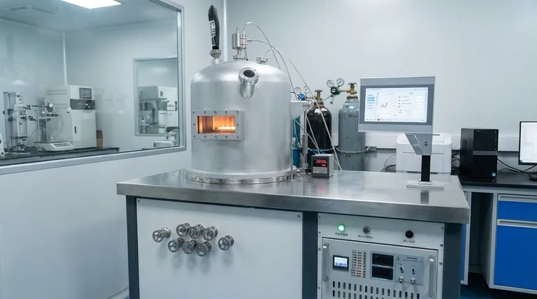
- Multi Heating Zones CVD Tube Furnace Machine Chemical Vapor Deposition Chamber System Equipment
- CVD Diamond Domes for Industrial and Scientific Applications
- CVD Diamond for Thermal Management Applications
- Chemical Vapor Deposition CVD Equipment System Chamber Slide PECVD Tube Furnace with Liquid Gasifier PECVD Machine
People Also Ask
- What color diamonds are CVD? Understanding the Process from Brown Tint to Colorless Beauty
- Can CVD diamonds change color? No, their color is permanent and stable.
- What is chemical vapor deposition of diamond? Grow High-Purity Diamonds Atom-by-Atom
- How long does it take to make synthetic diamonds? Discover the 6-8 Week Science Behind Lab-Grown Gems
- What is CVD diamond? The Ultimate Guide to Lab-Grown Diamonds and Their Uses


