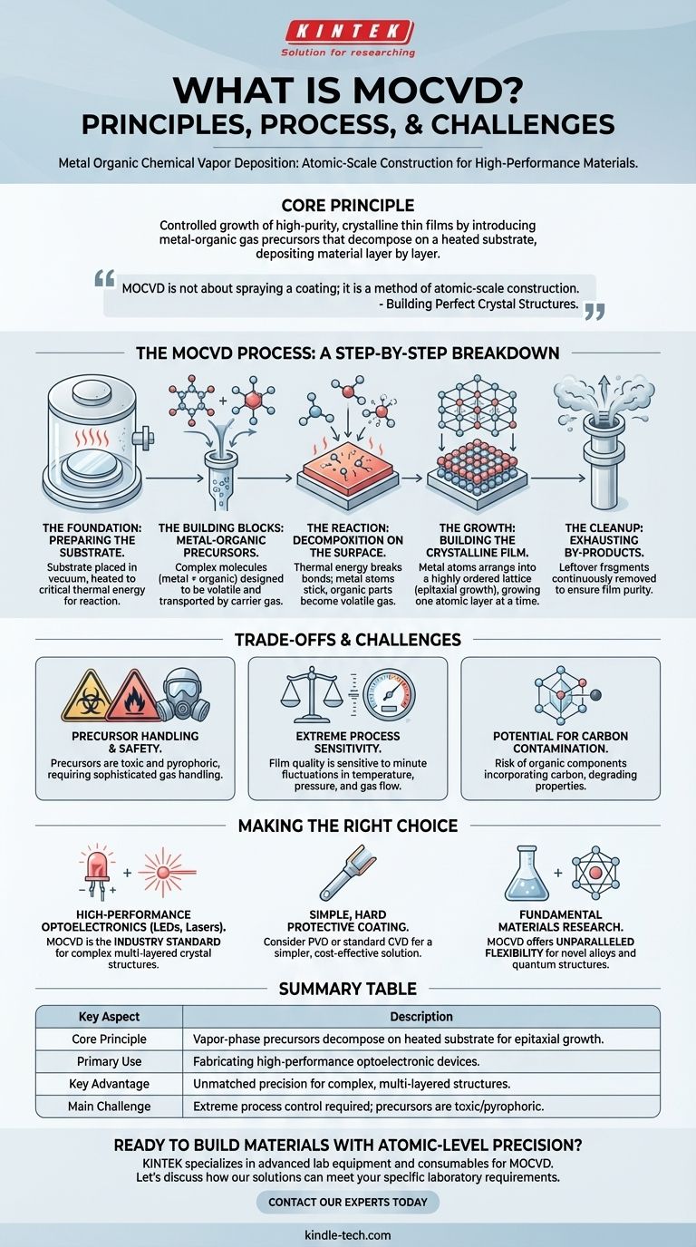
At its core, Metal Organic Chemical Vapor Deposition (MOCVD) is a highly controlled process for growing high-purity, crystalline thin films on a substrate. It involves introducing specific gaseous chemical precursors, known as metal-organics, into a reaction chamber. These gases decompose on a heated substrate, depositing a solid material layer by layer while volatile by-products are removed.
MOCVD is not about spraying a coating; it is a method of atomic-scale construction. By precisely controlling temperature, pressure, and gas flow, we orchestrate a chemical reaction on a surface to build perfect crystal structures, forming the foundation for high-performance electronic and optoelectronic devices.

The MOCVD Process: A Step-by-Step Breakdown
To understand the principle of MOCVD, it is best to view it as a sequence of carefully engineered events. Each step is critical for achieving a high-quality, uniform film.
The Foundation: Preparing the Substrate
The entire process begins with a substrate, which is the material upon which the film will be grown. This substrate is placed inside a reaction chamber, which is typically held under vacuum.
The substrate is then heated to a precise temperature. This heat is not for melting anything; it provides the critical thermal energy required to drive the chemical reaction on the surface.
The Building Blocks: Metal-Organic Precursors
The "Metal-Organic" in MOCVD refers to the precursor chemicals used. These are complex molecules where a central metal atom is bonded to organic molecules.
These compounds are specifically designed to be volatile, meaning they can easily be turned into a gas and transported into the reaction chamber with a carrier gas like hydrogen or nitrogen.
The Reaction: Decomposition on the Surface
When the precursor gases flow over the hot substrate, the thermal energy breaks the chemical bonds within the precursor molecules.
The metal atoms "stick" to the surface, while the now-detached organic components form new, volatile gaseous molecules. This is the core deposition event.
The Growth: Building the Crystalline Film
The deposited metal atoms do not land randomly. They arrange themselves into a highly ordered, crystalline lattice, often continuing the crystal structure of the underlying substrate. This process is known as epitaxial growth.
By continuously supplying the precursor gases, this film grows one atomic layer at a time, resulting in an exceptionally pure and structurally perfect material.
The Cleanup: Exhausting By-products
The leftover organic fragments and other reaction by-products remain in a gaseous state. These waste gases are continuously removed from the reaction chamber by the gas flow and vacuum system.
This constant removal is crucial for ensuring the purity of the growing film, preventing contamination from unwanted chemical residue.
Understanding the Trade-offs and Challenges
While powerful, MOCVD is a complex process with specific challenges that dictate its use. Understanding these trade-offs is key to appreciating its role.
Precursor Handling and Safety
The metal-organic precursors are often highly toxic and pyrophoric, meaning they can ignite spontaneously upon contact with air. This necessitates sophisticated, expensive gas handling and safety systems.
Extreme Process Sensitivity
The quality of the final film is exquisitely sensitive to minute fluctuations in temperature, pressure, and gas flow. Maintaining perfect uniformity across a large substrate is a major engineering challenge that requires highly advanced equipment.
Potential for Carbon Contamination
Because the precursors are "organic"—containing carbon-hydrogen bonds—there is an inherent risk that carbon atoms can be unintentionally incorporated into the film. This contamination can degrade the material's desired electronic or optical properties.
Making the Right Choice for Your Goal
Selecting MOCVD is a decision driven by the uncompromising need for material perfection.
- If your primary focus is high-performance optoelectronics (LEDs, lasers, solar cells): MOCVD is the industry standard due to its unmatched ability to create complex, multi-layered crystal structures with precise compositional control.
- If your primary focus is producing a simple, hard protective coating: A less complex and more cost-effective process like general Physical Vapor Deposition (PVD) or standard CVD is likely a better fit.
- If your primary focus is fundamental materials research: MOCVD offers unparalleled flexibility to create novel alloys and quantum structures by simply adjusting the mixture and flow of different precursor gases.
Ultimately, MOCVD is the definitive choice when the goal is to build a material with atomic-level precision.
Summary Table:
| Key Aspect | Description |
|---|---|
| Core Principle | Vapor-phase metal-organic precursors decompose on a heated substrate for epitaxial growth. |
| Primary Use | Fabricating high-performance optoelectronic devices (LEDs, lasers, solar cells). |
| Key Advantage | Unmatched precision for creating complex, multi-layered crystal structures. |
| Main Challenge | Requires extreme control of temperature, pressure, and gas flow; precursors are often toxic/pyrophoric. |
Ready to build materials with atomic-level precision?
KINTEK specializes in providing the advanced lab equipment and consumables necessary for sophisticated processes like Metal Organic Chemical Vapor Deposition (MOCVD). Whether you are developing next-generation LEDs, laser diodes, or high-efficiency solar cells, our expertise supports your need for high-purity materials and precise process control.
Let's discuss how our solutions can meet your specific laboratory requirements.
Contact our experts today to explore the right tools for your groundbreaking work.
Visual Guide
Related Products
- Multi Heating Zones CVD Tube Furnace Machine Chemical Vapor Deposition Chamber System Equipment
- 915MHz MPCVD Diamond Machine Microwave Plasma Chemical Vapor Deposition System Reactor
- Microwave Plasma Chemical Vapor Deposition MPCVD Machine System Reactor for Lab and Diamond Growth
- Cylindrical Resonator MPCVD Machine System Reactor for Microwave Plasma Chemical Vapor Deposition and Lab Diamond Growth
- Molybdenum Vacuum Heat Treat Furnace
People Also Ask
- What is the function of a high-temperature CVD tube furnace in 3D graphene foam prep? Master 3D Nanomaterial Growth
- What is the difference between hot wall CVD and cold wall CVD? Choose the Right System for Your Process
- What are the differences between chemical vapour deposition processes? A Guide to Pressure, Quality & Cost
- What are the advantages of a multi-zone tube furnace for Sb2S3? Unlock Superior Semiconductor Thin Film Purity
- What is a CVD tube furnace? A Complete Guide to Thin-Film Deposition