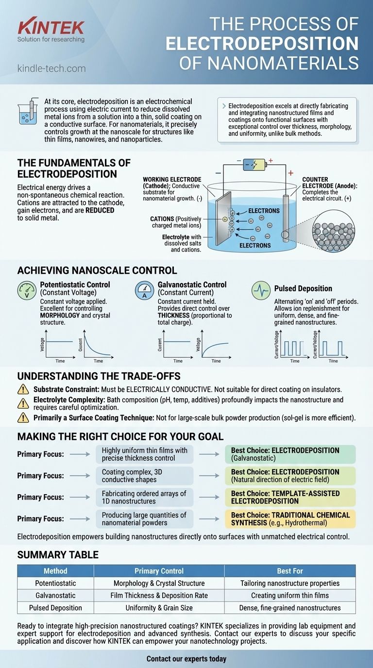
At its core, electrodeposition is an electrochemical process that uses an electric current to reduce dissolved metal ions from a solution, causing them to form a thin, solid coating onto a conductive surface. For nanomaterials, this technique is refined to precisely control the growth of this coating at the nanoscale, allowing for the creation of structures like thin films, nanowires, and nanoparticles with specific properties. It is a powerful alternative to traditional chemical synthesis routes like hydrothermal or sol-gel methods.
While many methods can produce nanomaterials in bulk powders or solutions, electrodeposition excels at directly fabricating and integrating nanostructured films and coatings onto functional surfaces with exceptional control over thickness, morphology, and uniformity.
The Fundamentals of Electrodeposition
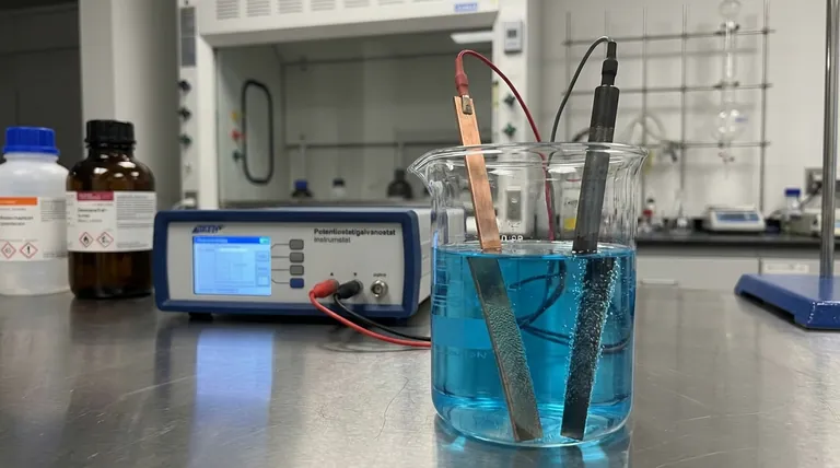
Electrodeposition functions like a highly controlled, miniature plating system. The process takes place within an electrochemical cell, where electrical energy drives a chemical reaction that would not otherwise occur spontaneously.
The Electrochemical Cell
The setup consists of three key components immersed in a solution.
- Working Electrode (Cathode): This is the conductive substrate where you want to grow your nanomaterial. It is connected to the negative terminal of a power source.
- Counter Electrode (Anode): This electrode completes the electrical circuit. It is connected to the positive terminal.
- Electrolyte: This is a solution containing dissolved salts of the material you wish to deposit (e.g., copper sulfate for depositing copper). These salts provide the metal ions that will form the nanomaterial.
The Deposition Mechanism
When a voltage is applied, the positively charged metal ions (cations) in the electrolyte are attracted to the negatively charged working electrode. At the surface of this electrode, the ions gain electrons and are reduced to their solid, metallic state.
This process is essentially "painting with ions," where the electric current dictates the rate and structure of the deposition, atom by atom or layer by layer.
Achieving Nanoscale Control
The key advantage of electrodeposition for nanomaterials is the ability to manipulate the growth by precisely controlling the electrical parameters. This is not easily achievable with purely chemical methods.
Potentiostatic Control (Constant Voltage)
In this mode, a constant voltage is applied. The initial current is high as ions rush to the surface, but it decreases as the ion concentration near the electrode depletes. This method is excellent for controlling the morphology and crystal structure of the deposit.
Galvanostatic Control (Constant Current)
Here, the current is held constant, ensuring a steady rate of material deposition. The system adjusts the voltage as needed to maintain this current. This mode provides direct control over the thickness of the deposited film, as thickness is proportional to the total charge passed.
Pulsed Deposition
Instead of a constant current or voltage, short pulses are used. This technique involves alternating between an "on" period where deposition occurs and an "off" period where no deposition happens. This "off" time allows ions in the solution to replenish near the electrode surface, leading to more uniform, dense, and fine-grained nanostructures.
Understanding the Trade-offs
While powerful, electrodeposition is not a universal solution. Understanding its limitations is crucial for making an informed decision.
The Substrate Constraint
The most significant limitation is that the substrate must be electrically conductive. This makes it unsuitable for directly coating insulating materials like glass or most polymers without first applying a thin conductive seed layer.
Electrolyte Complexity
The composition of the electrolyte—including pH, temperature, additives, and ion concentration—has a profound impact on the final nanostructure. Formulating and maintaining a stable bath can be complex and requires careful optimization for reproducible results.
Primarily a Surface Coating Technique
Electrodeposition is fundamentally a method for modifying surfaces or creating thin films. It is not designed for the large-scale, bulk production of nanomaterial powders, where methods like sol-gel or ball milling are more efficient.
Making the Right Choice for Your Goal
Selecting a synthesis method depends entirely on your end goal. Electrodeposition offers a unique set of capabilities tailored for specific applications.
- If your primary focus is creating highly uniform thin films with precise thickness control: Electrodeposition, particularly in galvanostatic mode, is an exceptional choice due to its direct, real-time control over deposition rate.
- If your primary focus is coating complex, three-dimensional conductive shapes: Electrodeposition is highly effective as the electric field naturally directs deposition onto all conductive surfaces, even those with intricate geometries.
- If your primary focus is fabricating ordered arrays of 1D nanostructures like nanowires or nanotubes: Template-assisted electrodeposition, where a porous membrane acts as a mold, is a dominant and highly successful technique.
- If your primary focus is producing large quantities of nanomaterial powders: Traditional chemical synthesis routes like hydrothermal methods or co-precipitation are often more scalable and cost-effective.
Ultimately, electrodeposition empowers you to build nanostructured materials directly onto a functional surface with a level of electrical control that other methods cannot match.
Summary Table:
| Method | Primary Control | Best For |
|---|---|---|
| Potentiostatic (Constant Voltage) | Morphology & Crystal Structure | Tailoring nanostructure properties |
| Galvanostatic (Constant Current) | Film Thickness & Deposition Rate | Creating uniform thin films |
| Pulsed Deposition | Uniformity & Grain Size | Dense, fine-grained nanostructures |
Ready to integrate high-precision nanostructured coatings into your research or product development?
KINTEK specializes in providing the lab equipment and expert support you need to successfully implement electrodeposition and other advanced material synthesis techniques. Our team can help you select the right tools and optimize your process for superior results.
Contact our experts today to discuss your specific application and discover how KINTEK can empower your nanotechnology projects.
Visual Guide
Related Products
- HFCVD Machine System Equipment for Drawing Die Nano-Diamond Coating
- RF PECVD System Radio Frequency Plasma-Enhanced Chemical Vapor Deposition RF PECVD
- Electron Beam Evaporation Coating Oxygen-Free Copper Crucible and Evaporation Boat
- Chemical Vapor Deposition CVD Equipment System Chamber Slide PECVD Tube Furnace with Liquid Gasifier PECVD Machine
- Electrode Polishing Material for Electrochemical Experiments
People Also Ask
- What is the full form of HFCVD? A Guide to Hot Filament Chemical Vapor Deposition
- What are the disadvantages and challenges of the HFCVD method? Overcome Growth Limits and Filament Issues
- How expensive is chemical vapor deposition? Understanding the True Cost of High-Performance Coating
- What is the function of tungsten filaments in HFCVD? Powering Diamond Film Synthesis with Thermal Excitation
- What types of substrates are used in CVD to facilitate graphene films? Optimize Graphene Growth with the Right Catalyst