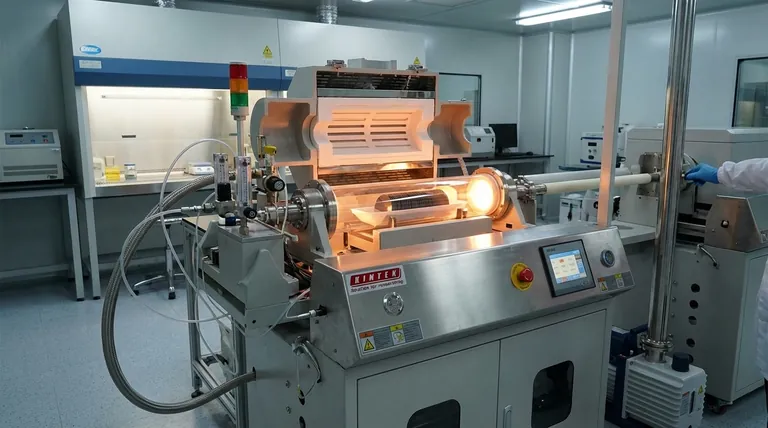
In short, Low-Pressure Chemical Vapor Deposition (LPCVD) is a process that creates a solid, high-purity thin film on a material's surface (known as a substrate). It works by introducing reactive precursor gases into a chamber at very low pressure and high temperature. The heat causes the gases to react and decompose, depositing a uniform layer of the desired material onto the heated substrate.
The critical insight is that operating at low pressure significantly increases the uniformity of the deposited film. This allows LPCVD to coat complex, three-dimensional surfaces and to process many substrates at once with exceptional consistency.
The Foundational Process: Chemical Vapor Deposition (CVD)
Before understanding the "low-pressure" advantage, we must first grasp the core mechanism of Chemical Vapor Deposition (CVD), which forms the basis for the LPCVD process.
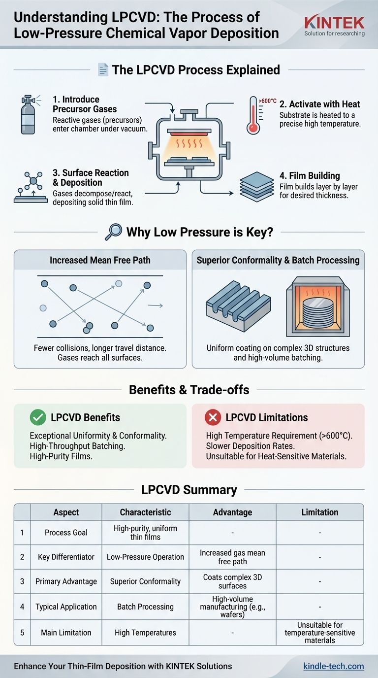
Step 1: Introducing Precursor Gases
The process begins by feeding specific volatile gases, known as precursors, into a reaction chamber that is under vacuum. These gases contain the chemical elements that will make up the final thin film.
Step 2: Activating the Reaction with Heat
Inside the chamber, one or more substrates are heated to a precise reaction temperature. This thermal energy is the catalyst for the entire process.
Step 3: Deposition on the Substrate
When the precursor gases come into contact with the hot substrate surface, they undergo a chemical reaction or decompose. This reaction forms a nonvolatile, solid material that bonds directly to the substrate, creating the thin film.
Step 4: Building the Film
Over time, this deposition process continues, building up the film layer by layer. The result is a highly pure and often crystalline or amorphous solid material evenly distributed across the substrate.
Why Low Pressure is the Key Differentiator
Operating the CVD process at low pressure (LPCVD) is not a minor adjustment; it fundamentally changes the physics of the deposition and provides distinct, powerful advantages.
Increased Mean Free Path
At low pressure, there are far fewer gas molecules in the chamber. This dramatically increases the mean free path—the average distance a gas molecule can travel before colliding with another.
This longer path means the precursor molecules are more likely to reach every nook and cranny of the substrate before reacting, rather than reacting in the gas phase.
Superior Conformality
The direct result of an increased mean free path is exceptional conformality. The film deposits evenly not just on flat surfaces but also over steps, into trenches, and around complex 3D structures.
This is a key advantage over line-of-sight deposition methods like Physical Vapor Deposition (PVD).
High-Throughput Batch Processing
The excellent uniformity of LPCVD allows for substrates to be stacked vertically in a furnace, very close to one another.
Because the gas can effectively penetrate the spaces between them, hundreds of wafers or components can be coated simultaneously in a single "batch," making the process highly efficient for manufacturing.
Understanding the Trade-offs
While powerful, LPCVD is not the solution for every application. Its primary limitations are tied directly to its reliance on thermal energy.
High-Temperature Requirement
LPCVD processes typically require very high temperatures (often >600°C) to drive the necessary chemical reactions.
This high heat can damage or alter underlying materials or devices already fabricated on the substrate, making it unsuitable for temperature-sensitive applications.
Slower Deposition Rates
The process is generally limited by the rate of the surface reaction. Compared to other methods like atmospheric pressure CVD (APCVD), the deposition rates for LPCVD are often lower.
This makes it less ideal for applications requiring very thick films where speed is the dominant concern.
Making the Right Choice for Your Goal
Selecting a deposition method depends entirely on the required properties of the final film and the constraints of your substrate.
- If your primary focus is exceptional uniformity and conformal coating on complex surfaces: LPCVD is the superior choice due to its low-pressure operation.
- If your primary focus is high-volume manufacturing throughput: The batch processing capability of LPCVD makes it a highly cost-effective and efficient solution.
- If your substrate cannot tolerate high temperatures: You must consider alternative methods like Plasma-Enhanced CVD (PECVD), which uses plasma energy to enable reactions at much lower temperatures.
Ultimately, understanding the interplay between pressure, temperature, and gas transport is the key to mastering thin-film deposition.
Summary Table:
| Key Aspect | LPCVD Characteristic |
|---|---|
| Process Goal | Deposit high-purity, uniform thin films on a substrate |
| Key Differentiator | Operates at low pressure for increased gas mean free path |
| Primary Advantage | Superior conformality and uniformity on complex 3D structures |
| Typical Application | High-throughput batch processing of multiple substrates (e.g., wafers) |
| Main Limitation | Requires high temperatures (>600°C), unsuitable for temperature-sensitive materials |
Need a High-Purity, Uniform Thin Film for Your Application?
KINTEK specializes in providing advanced lab equipment and consumables for precise thin-film deposition processes like LPCVD. Whether you are developing semiconductor devices, MEMS, or advanced coatings, our solutions help you achieve exceptional film uniformity and conformality on even the most complex 3D surfaces.
Contact our experts today to discuss how our LPCVD systems and support can enhance your laboratory's capabilities and manufacturing throughput.
Visual Guide
Related Products
- Chemical Vapor Deposition CVD Equipment System Chamber Slide PECVD Tube Furnace with Liquid Gasifier PECVD Machine
- Inclined Rotary Plasma Enhanced Chemical Vapor Deposition PECVD Equipment Tube Furnace Machine
- RF PECVD System Radio Frequency Plasma-Enhanced Chemical Vapor Deposition RF PECVD
- Microwave Plasma Chemical Vapor Deposition MPCVD Machine System Reactor for Lab and Diamond Growth
- 915MHz MPCVD Diamond Machine Microwave Plasma Chemical Vapor Deposition System Reactor
People Also Ask
- How expensive is chemical vapor deposition? Understanding the True Cost of High-Performance Coating
- What are the core advantages of PE-CVD in OLED encapsulation? Protect Sensitive Layers with Low-Temp Film Deposition
- What is plasma enhanced chemical vapor deposition PECVD equipment? A Guide to Low-Temperature Thin Film Deposition
- How are carbon nanotubes grown? Master Scalable Production with Chemical Vapor Deposition
- What happens during deposition chemistry? Building Thin Films from Gaseous Precursors


