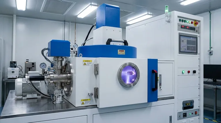
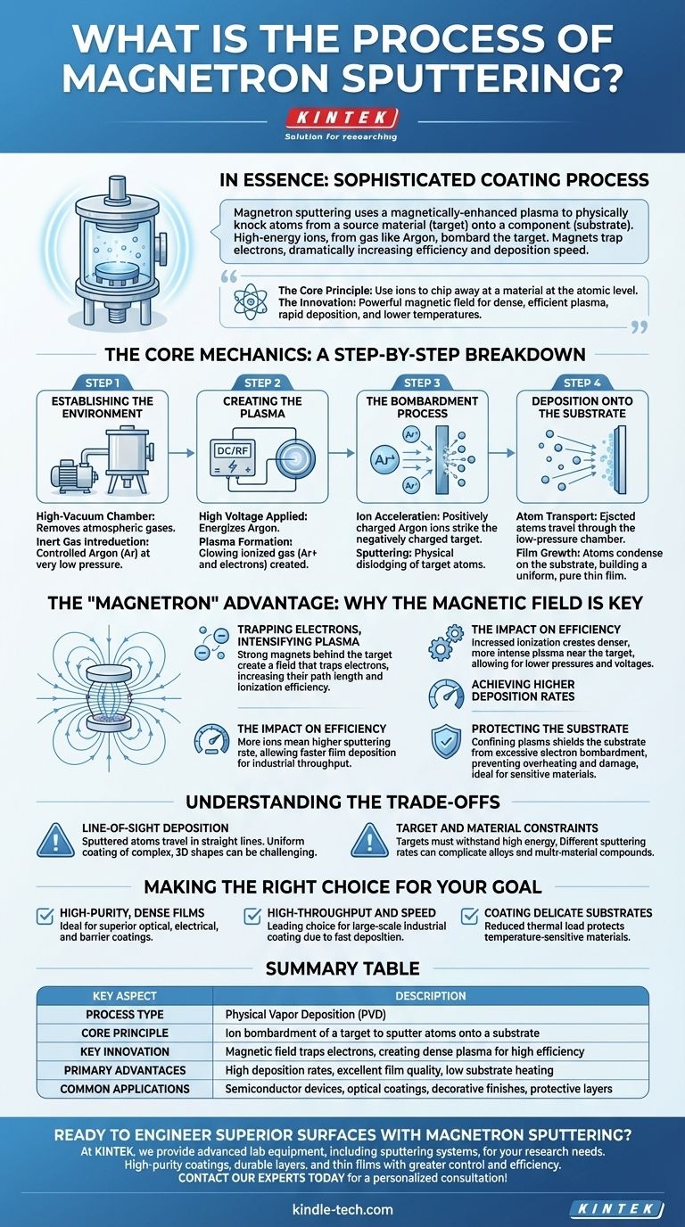
In essence, magnetron sputtering is a sophisticated coating process that uses a magnetically-enhanced plasma to physically knock atoms from a source material (the "target") onto a component (the "substrate"). High-energy ions, generated from a gas like argon, bombard the target. The magnetic field's critical role is to trap electrons near the target, dramatically increasing the efficiency of the plasma and allowing for faster, more controlled deposition of a thin film.
The core principle is simple: use ions to chip away at a material at the atomic level. The innovation of magnetron sputtering, however, lies in using a powerful magnetic field to create a dense, highly efficient plasma, enabling rapid deposition of high-quality films at lower temperatures and pressures than other methods.
The Core Mechanics: A Step-by-Step Breakdown
To truly understand magnetron sputtering, it's best to visualize it as a sequence of controlled events occurring within a highly engineered environment.
Step 1: Establishing the Environment
The entire process takes place inside a high-vacuum chamber. This is critical because it removes atmospheric gases that could contaminate the film or interfere with the process.
Once a vacuum is achieved, a small, controlled amount of an inert gas, most commonly argon (Ar), is introduced into the chamber at a very low pressure.
Step 2: Creating the Plasma
A high DC or RF voltage is applied across the chamber. The material to be deposited, known as the target, is set up as the cathode (negatively charged).
This strong electric field energizes the argon gas, stripping electrons from the argon atoms. This creates a mixture of positively charged argon ions (Ar+) and free electrons, forming a glowing, ionized gas called a plasma or "glow discharge."
Step 3: The Bombardment Process
The positively charged argon ions are powerfully accelerated by the electric field toward the negatively charged target.
These ions collide with the target surface with such force that they physically dislodge, or "sputter," individual atoms of the target material.
Step 4: Deposition onto the Substrate
The ejected atoms from the target travel through the low-pressure chamber. They eventually strike the component being coated, known as the substrate.
Upon arrival, these atoms condense on the substrate's surface, gradually building up a uniform, thin, and highly pure film.
The "Magnetron" Advantage: Why the Magnetic Field is Key
The process described above is simple sputtering. Adding a magnetic field—transforming it into magnetron sputtering—is what makes the technique so powerful and widely used.
Trapping Electrons, Intensifying Plasma
Strong magnets are placed behind the target. This creates a magnetic field that traps the lighter, negatively charged electrons in a looping path directly in front of the target's surface.
Without this field, electrons would be lost to the chamber walls. By trapping them, their path length is greatly increased, which means they are far more likely to collide with and ionize neutral argon atoms.
The Impact on Efficiency
This increased ionization creates a much denser, more intense plasma that is concentrated right where it is needed most: near the target.
This allows the sputtering process to be sustained at much lower gas pressures and voltages, increasing overall process stability and control.
Achieving Higher Deposition Rates
A denser plasma means there are significantly more positive argon ions available to bombard the target. This directly results in a much higher sputtering rate, allowing films to be deposited faster.
This increase in speed is a primary reason magnetron sputtering is favored for industrial and high-throughput applications.
Protecting the Substrate
By confining the plasma and electrons near the target, the substrate is shielded from excessive electron bombardment. This prevents overheating and potential damage, making the process ideal for coating temperature-sensitive materials like plastics and polymers.
Understanding the Trade-offs
No technology is without its limitations, and being an effective advisor means acknowledging them.
Line-of-Sight Deposition
Sputtering is fundamentally a line-of-sight process. The sputtered atoms travel in relatively straight lines from the target to the substrate.
This can make it challenging to uniformly coat complex, three-dimensional shapes with deep recesses or undercuts without sophisticated substrate rotation.
Target and Material Constraints
The target material must be fabricated into a specific shape and must be able to withstand the high-energy ion bombardment and thermal load.
Some materials sputter at very different rates than others, which can complicate the deposition of alloy films or compounds from multiple targets.
Making the Right Choice for Your Goal
Magnetron sputtering is not a one-size-fits-all solution. Its value is tied directly to the specific outcome you need to achieve.
- If your primary focus is high-purity, dense films: The low-pressure, high-vacuum environment is ideal for creating superior optical, electrical, or barrier coatings.
- If your primary focus is high-throughput and speed: The high deposition rates enabled by the magnetic field make this a leading choice for large-scale industrial coating.
- If your primary focus is coating delicate substrates: The reduced thermal load protects temperature-sensitive materials that would be damaged by other deposition methods.
Ultimately, magnetron sputtering provides an exceptional level of control for engineering surfaces at the atomic level to achieve specific functional properties.
Summary Table:
| Key Aspect | Description |
|---|---|
| Process Type | Physical Vapor Deposition (PVD) |
| Core Principle | Ion bombardment of a target material to sputter atoms onto a substrate. |
| Key Innovation | Magnetic field traps electrons, creating a dense plasma for high efficiency. |
| Primary Advantages | High deposition rates, excellent film quality, low substrate heating. |
| Common Applications | Semiconductor devices, optical coatings, decorative finishes, protective layers. |
Ready to Engineer Superior Surfaces with Magnetron Sputtering?
At KINTEK, we specialize in providing advanced lab equipment, including sputtering systems, to meet the precise needs of your research and development. Whether you require high-purity coatings for semiconductors, durable layers for optics, or thin films for innovative materials, our expertise can help you achieve your goals with greater control and efficiency.
Let's discuss how our solutions can enhance your laboratory's capabilities. Contact our experts today for a personalized consultation!
Visual Guide
Related Products
- Microwave Plasma Chemical Vapor Deposition MPCVD Machine System Reactor for Lab and Diamond Growth
- Chemical Vapor Deposition CVD Equipment System Chamber Slide PECVD Tube Furnace with Liquid Gasifier PECVD Machine
- Molybdenum Tungsten Tantalum Special Shape Evaporation Boat
- Inclined Rotary Plasma Enhanced Chemical Vapor Deposition PECVD Equipment Tube Furnace Machine
- Inclined Rotary Plasma Enhanced Chemical Vapor Deposition PECVD Equipment Tube Furnace Machine
People Also Ask
- What is microwave plasma chemical vapor deposition? A Guide to High-Purity Diamond Film Growth
- What are the primary advantages of the CVD method for growing diamonds? Engineering High-Purity Gems and Components
- How do vacuum pumps and valves collaborate in MPCVD? Achieve Precise Pressure Control for Superior CNT Synthesis
- How does a microwave plasma reactor facilitate the synthesis of diamond? Master MPCVD with Precision Technology
- Why is argon-rich gas phase chemistry used for UNCD growth? Unlock Precision Nano-Diamond Synthesis