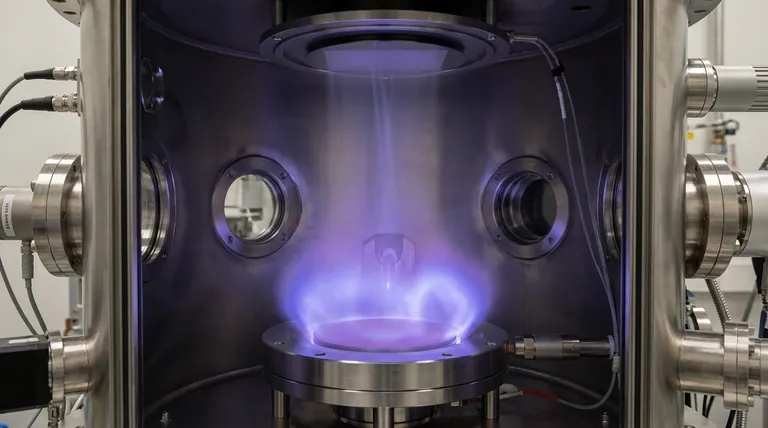
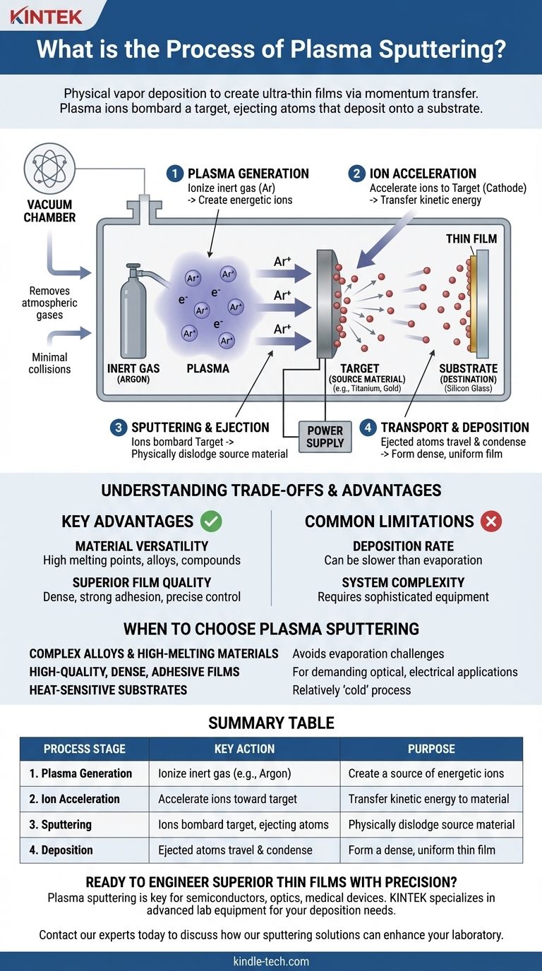
In short, plasma sputtering is a physical vapor deposition process used to create ultra-thin films. It works by creating a plasma in a vacuum, accelerating ions from that plasma to strike a source material (the "target"), and physically knocking atoms off the target, which then travel and deposit onto a substrate as a uniform coating.
Sputtering is fundamentally a momentum transfer process. Unlike methods that melt materials, it uses energetic ions as atomic-scale projectiles to chip away at a source, offering exceptional control over the composition and structure of the deposited thin film.
Deconstructing the Sputtering Environment
To understand the process, we must first understand the key components and conditions within the sputtering chamber. Each element plays a critical role in the final outcome.
The Vacuum Chamber
The entire process occurs in a high-vacuum chamber. This is crucial for two reasons: it removes atmospheric gases that could contaminate the film, and it allows the sputtered atoms to travel from the target to the substrate with minimal collisions.
The Inert Gas (Typically Argon)
The chamber is backfilled with a small, controlled amount of an inert gas, most commonly Argon (Ar). This gas is not part of the final film; its sole purpose is to be ionized to create the plasma that drives the process.
The Target (The Source Material)
The target is a solid piece of the material you wish to deposit as a thin film (e.g., titanium, gold, silicon dioxide). It is connected to a power supply and acts as the cathode (negative electrode) in the plasma circuit.
The Substrate (The Destination)
The substrate is the object being coated, such as a silicon wafer, glass panel, or medical implant. It is positioned to face the target, ready to receive the stream of sputtered atoms.
The Core Mechanism: From Plasma to Film
The sputtering process is a precise, four-step sequence that leverages plasma physics and kinetic energy.
Step 1: Plasma Generation
A high voltage is applied to the target. This electrical energy strips electrons from some of the Argon atoms, creating a mixture of free electrons and positively charged Argon ions (Ar+). This energized, ionized gas is a plasma.
Step 2: Ion Acceleration and Bombardment
The positively charged Argon ions are forcefully accelerated toward the negatively charged target. They are drawn by the strong electric field, much like a magnet pulling on a piece of metal.
Step 3: Sputtering and Ejection
The Argon ions collide with the target surface with significant kinetic energy. This impact is powerful enough to overcome the atomic binding forces of the target material, physically knocking atoms or molecules loose. This ejection of material is the "sputtering" effect.
Step 4: Transport and Deposition
The ejected target atoms travel in a vapor stream across the vacuum chamber. When they reach the substrate, they condense on its surface, gradually building up layer by layer to form a dense, uniform thin film.
Understanding the Trade-offs and Advantages
Sputtering is a powerful technique, but it's essential to understand its specific strengths and weaknesses compared to other deposition methods like Chemical Vapor Deposition (CVD) or thermal evaporation.
Key Advantage: Material Versatility
Because sputtering is a physical and not a thermal process, it is exceptionally good at depositing materials with very high melting points. It is also ideal for depositing alloys and compounds, as it preserves the original material's composition (stoichiometry) in the final film.
Key Advantage: Superior Film Quality
The energetic nature of the sputtered atoms results in films that are typically very dense, have strong adhesion to the substrate, and offer precise control over thickness and uniformity across large areas.
Common Limitation: Deposition Rate
Sputtering can be slower than other methods like thermal evaporation, which can be a factor in high-volume manufacturing where throughput is a primary concern.
Common Limitation: System Complexity
Sputtering systems require a sophisticated combination of high-vacuum pumps, high-voltage power supplies, and gas flow controllers, making the equipment more complex and costly than simpler deposition techniques.
When to Choose Plasma Sputtering
Your choice of deposition method depends entirely on the requirements of your final product. Sputtering is often the superior choice for high-performance applications.
- If your primary focus is depositing complex alloys or high-melting-point materials: Sputtering is the ideal method, as it avoids the challenges of evaporation and maintains material composition.
- If your primary focus is achieving high-quality, dense, and adhesive films: The energetic deposition mechanism of sputtering provides excellent film properties for demanding optical, electrical, or mechanical applications.
- If your primary focus is coating heat-sensitive substrates: Sputtering is a relatively "cold" process compared to thermal evaporation, minimizing the risk of thermal damage to substrates like plastics.
By controlling the physics of momentum transfer at the atomic level, sputtering empowers you to engineer materials with precision.
Summary Table:
| Process Stage | Key Action | Purpose |
|---|---|---|
| 1. Plasma Generation | Ionize inert gas (e.g., Argon) | Create a source of energetic ions |
| 2. Ion Acceleration | Accelerate ions toward target (cathode) | Transfer kinetic energy to target material |
| 3. Sputtering | Ions bombard target, ejecting atoms | Physically dislodge source material |
| 4. Deposition | Ejected atoms travel & condense on substrate | Form a dense, uniform thin film |
Ready to Engineer Superior Thin Films with Precision?
Plasma sputtering is the key to depositing high-quality, uniform coatings for demanding applications in semiconductors, optics, and medical devices. The right equipment is critical for success.
KINTEK specializes in advanced lab equipment and consumables for all your deposition needs. Our expertise ensures you achieve the precise film properties your research or production requires.
Contact our experts today to discuss how our sputtering solutions can enhance your laboratory's capabilities and drive your projects forward.
Visual Guide
Related Products
- Spark Plasma Sintering Furnace SPS Furnace
- Chemical Vapor Deposition CVD Equipment System Chamber Slide PECVD Tube Furnace with Liquid Gasifier PECVD Machine
- RF PECVD System Radio Frequency Plasma-Enhanced Chemical Vapor Deposition RF PECVD
- Microwave Plasma Chemical Vapor Deposition MPCVD Machine System Reactor for Lab and Diamond Growth
- 915MHz MPCVD Diamond Machine Microwave Plasma Chemical Vapor Deposition System Reactor
People Also Ask
- What is the difference between spark plasma sintering and flash sintering? A Guide to Advanced Sintering Methods
- What is the pressure for spark plasma sintering? A Guide to Optimizing SPS Parameters
- What technical advantages does a Spark Plasma Sintering (SPS) furnace offer for LZP ceramics? Enhance Ionic Conductivity
- What are the advantages of CAMI/SPS for W-Cu composite preparation? Reduce cycles from hours to seconds.
- What is the theory of spark plasma sintering? A Guide to Rapid, Low-Temperature Densification


