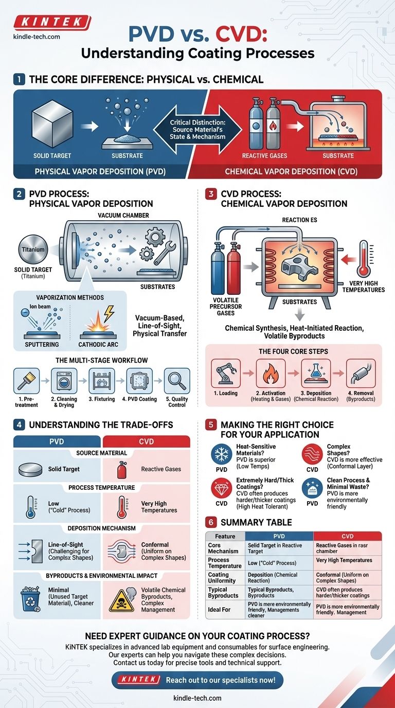
In essence, the core difference is physical versus chemical. Physical Vapor Deposition (PVD) is a vacuum-based process where a solid material is vaporized and then physically deposited onto a part, atom by atom. Conversely, Chemical Vapor Deposition (CVD) uses reactive gases that undergo a chemical reaction at the part's heated surface, forming a new material layer from the resulting chemical breakdown.
The critical distinction lies in the source material's state: PVD physically transfers a solid material into a vapor and onto a part, while CVD chemically builds a new layer from reactive gases. This fundamental difference in mechanism dictates the process conditions, resulting properties, and ideal applications for each coating.
The Physical Vapor Deposition (PVD) Process
PVD is fundamentally a line-of-sight deposition technique that occurs under a high vacuum. It is best understood as moving a material from a source target directly onto the substrate's surface without changing its chemical nature.
The Principle of Physical Transfer
The entire PVD process is carried out in a vacuum chamber to ensure the purity of the coating. A solid source material, known as a target (e.g., titanium, chromium), is the source of the coating.
Vaporization Methods
To transfer the target material, it must first be converted into a vapor. This is accomplished through high-energy methods, including:
- Sputtering: An ion beam (plasma) bombards the solid target, physically knocking atoms off its surface.
- Cathodic Arc: A high-current arc moves across the target's surface, vaporizing the material.
The vaporized metal then travels through the vacuum chamber and condenses on the cooler parts, creating a thin, strongly bonded film. Reactive gases like nitrogen can be introduced to create specific compounds like Titanium Nitride (TiN).
The Multi-Stage Workflow
A successful PVD coating involves more than just the deposition step. A typical industrial process includes:
- Pre-treatment: Stripping old coatings and preparing the surface.
- Cleaning & Drying: Ensuring the part is atomically clean for optimal adhesion.
- Fixturing: Mounting parts in the chamber for uniform exposure.
- PVD Coating: The vaporization and deposition process itself.
- Quality Control: Measuring thickness and inspecting for defects.
The Chemical Vapor Deposition (CVD) Process
CVD is not a physical transfer but a chemical synthesis that happens directly on the surface of the part. It relies on heat to initiate and sustain the reaction.
The Principle of Chemical Reaction
In CVD, various volatile precursor gases are introduced into a reaction chamber. The part to be coated (the substrate) is heated to a high temperature, providing the energy needed to trigger a chemical reaction between the gases.
The Four Core Steps
The CVD process follows a clear sequence:
- Loading: The substrate is placed inside the reaction chamber.
- Activation: The chamber is heated and pressure is adjusted while a mixture of precursor and inert gases is introduced.
- Deposition: The high temperature causes the gases to decompose and react on the substrate's surface, depositing a new, solid film.
- Removal: Volatile chemical byproducts from the reaction are pumped out of the chamber for safe processing.
Understanding the Trade-offs
The choice between PVD and CVD is dictated by the fundamental differences in their mechanisms and operating conditions.
Source Material: Solid vs. Gas
PVD uses a solid target of the coating material. CVD uses a precise mixture of reactive gases. This is the most foundational difference and influences the entire setup.
Process Temperature
This is the most significant practical distinction. PVD is a "cold" process, typically running at much lower temperatures. CVD requires very high temperatures to provide the activation energy for the chemical reactions.
Deposition Mechanism: Line-of-Sight vs. Conformal
Because PVD atoms travel in a straight line, it is considered a line-of-sight process. This can make it challenging to evenly coat complex, three-dimensional shapes.
CVD gases, however, can flow and diffuse into cavities and around corners, resulting in a highly uniform and conformal coating that covers all exposed surfaces evenly.
Byproducts and Environmental Impact
PVD is a cleaner process, with the primary "waste" being the unused target material. CVD inherently produces volatile chemical byproducts that must be carefully managed and treated, adding complexity to the operation.
Making the Right Choice for Your Application
Your final decision depends entirely on the material you are coating and the properties you need to achieve.
- If your primary focus is coating heat-sensitive materials: PVD is the superior choice due to its significantly lower operating temperatures, which won't damage or distort the underlying part.
- If your primary focus is a highly uniform coating on a complex shape: CVD is often more effective, as the precursor gases can reach all surfaces to create a conformal layer.
- If your primary focus is an extremely hard and wear-resistant coating: CVD can often produce thicker and harder coatings (like diamond-like carbon), assuming the substrate can tolerate the high heat.
- If your primary focus is a clean process with minimal chemical waste: PVD is the more straightforward and environmentally friendly option, as it does not produce volatile byproducts.
Understanding the core distinction between physical transfer and chemical reaction is the key to selecting the right surface engineering solution for your specific challenge.
Summary Table:
| Feature | PVD (Physical Vapor Deposition) | CVD (Chemical Vapor Deposition) |
|---|---|---|
| Core Mechanism | Physical transfer of vaporized solid material | Chemical reaction of gases on a heated surface |
| Process Temperature | Low ("cold" process) | Very High |
| Coating Uniformity | Line-of-sight (can struggle with complex shapes) | Conformal (excellent for complex 3D shapes) |
| Typical Byproducts | Minimal (unused target material) | Volatile chemical byproducts |
| Ideal For | Heat-sensitive materials, cleaner process | Complex shapes, extremely hard/thick coatings |
Need Expert Guidance on Your Coating Process?
Choosing between PVD and CVD is critical for achieving the desired performance, durability, and cost-efficiency for your components. The wrong choice can lead to part failure or unnecessary expense.
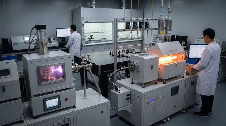
KINTEK specializes in advanced lab equipment and consumables for surface engineering. Our experts can help you navigate these complex decisions. We provide the precise tools and technical support needed for research, development, and quality control in coating applications.
Contact us today to discuss your specific requirements and discover how our solutions can enhance your coating process, improve product quality, and accelerate your time to market.
Reach out to our specialists now!
Visual Guide
Related Products
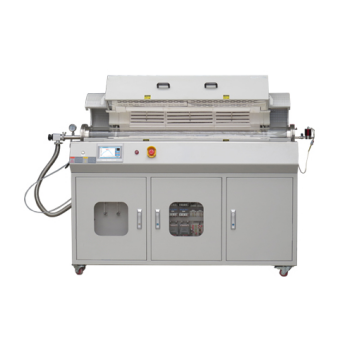
- Chemical Vapor Deposition CVD Equipment System Chamber Slide PECVD Tube Furnace with Liquid Gasifier PECVD Machine
- Inclined Rotary Plasma Enhanced Chemical Vapor Deposition PECVD Equipment Tube Furnace Machine
- RF PECVD System Radio Frequency Plasma-Enhanced Chemical Vapor Deposition RF PECVD
- Customer Made Versatile CVD Tube Furnace Chemical Vapor Deposition Chamber System Equipment
- Split Chamber CVD Tube Furnace with Vacuum Station Chemical Vapor Deposition System Equipment Machine
People Also Ask
- How plasma is generated in PECVD? A Step-by-Step Breakdown of the Process
- How is PECVD different from CVD? Unlock Low-Temperature Thin Film Deposition
- Why is PECVD better than CVD? Achieve Superior Low-Temperature Thin Film Deposition
- What is the difference between CVD and PVD process? A Guide to Choosing the Right Coating Method
- What is the difference between CVD and PECVD? Choose the Right Thin-Film Deposition Method