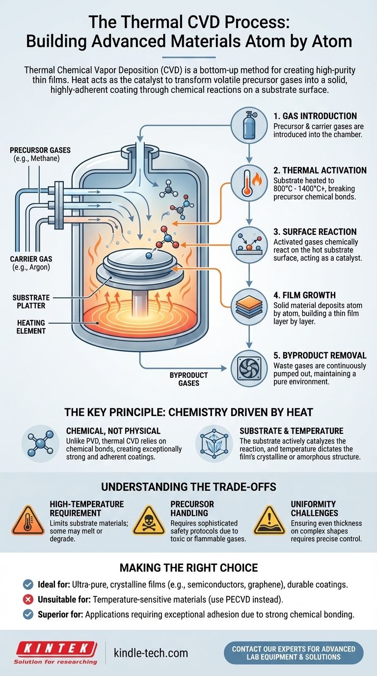
In its simplest terms, the process of thermal Chemical Vapor Deposition (CVD) is a method for building a solid, high-purity thin film on a surface from a gas. Precursor gases containing the required atoms are introduced into a high-temperature chamber, where they chemically react on a heated object (the substrate), depositing a solid layer atom by atom.
The core principle of thermal CVD is using heat as the catalyst to transform volatile gases into a solid, highly-adherent coating. It is a bottom-up manufacturing process where a material is literally constructed on a surface through controlled chemical reactions.
Deconstructing the Thermal CVD Process
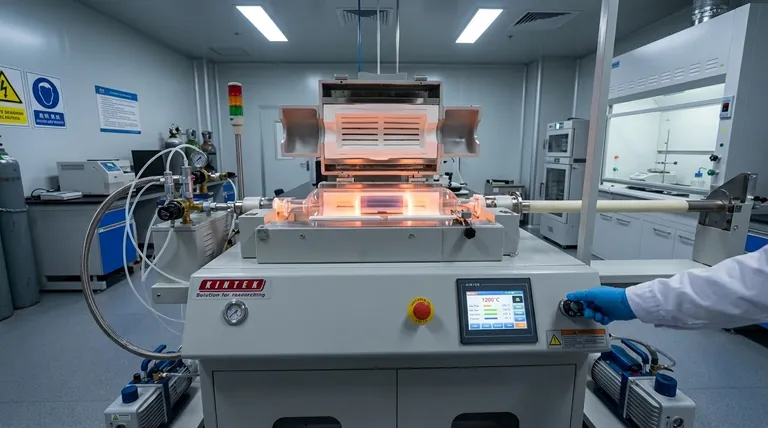
To truly understand thermal CVD, it's best to break it down into its fundamental components and sequential steps. The entire process occurs within a sealed, controlled reaction chamber.
The Core Components
- Substrate: This is the material or object that will be coated. It provides the surface where the chemical reactions take place and the film grows.
- Precursors: These are volatile gases that contain the chemical elements needed to create the desired film. For example, to grow a diamond film, a carbon-rich gas like methane (CH₄) is used.
- Heat Source: This provides the critical thermal energy required to initiate and sustain the chemical reactions on the substrate's surface.
Step 1: Introducing Precursor Gases
The process begins by feeding one or more precursor gases into the reaction chamber. Often, an inert carrier gas (like argon) is used to dilute the precursors and control their flow over the substrate.
Step 2: High-Temperature Activation
The substrate within the chamber is heated to a specific, high temperature, typically ranging from 800°C to over 1400°C. This intense heat provides the activation energy needed to break the chemical bonds within the precursor gas molecules.
Step 3: Reaction on the Substrate Surface
As the thermally-activated gas molecules make contact with the hot substrate, a chemical reaction occurs. The substrate's surface acts as a catalyst, providing an ideal site for the reactive gas species to settle and form new, stable chemical bonds.
Step 4: Film Growth and Deposition
This surface reaction results in the deposition of a solid material, forming a thin film. This process continues as more gas molecules react on the surface, causing the film to grow in thickness, often layer by layer, creating a highly ordered crystalline or amorphous structure.
Step 5: Removal of Byproducts
The chemical reactions produce waste gases as byproducts. These unreacted or byproduct gases are continuously removed from the chamber to maintain the purity of the environment and allow the deposition process to continue efficiently.
The Key Principle: Chemistry Driven by Heat
Understanding the "why" behind thermal CVD is crucial. Its effectiveness comes from the nature of the chemical bonds it creates.
It's a Chemical, Not Physical, Process
This is the most critical distinction. Unlike Physical Vapor Deposition (PVD), which uses physical processes like evaporation, thermal CVD relies on chemical reactions. The atoms of the film are chemically bonded to the substrate, creating an exceptionally strong and adherent coating.
The Substrate is an Active Participant
The substrate is not just a passive canvas. Its temperature and material composition actively catalyze the reaction. For example, when growing graphene, a copper substrate is often used because it both catalyzes the decomposition of carbon gases and provides an ideal surface for the graphene lattice to form.
Temperature Dictates the Outcome
Temperature is the primary control lever in thermal CVD. It governs the reaction rate and, most importantly, the final properties of the film. Different temperatures can result in either a highly ordered crystalline structure or a disordered amorphous one.
Understanding the Trade-offs
While powerful, thermal CVD is not without its limitations. Objectivity requires acknowledging them.
High-Temperature Requirement
The need for extreme heat is the primary constraint. It limits the types of substrates that can be used, as many materials would melt, warp, or degrade at the required operating temperatures.
Precursor Handling
The precursor gases used can be highly toxic, flammable, or corrosive. This necessitates sophisticated safety protocols and handling equipment, adding to the complexity and cost of the process.
Uniformity Challenges
While CVD generally produces very uniform (conformal) coatings, ensuring a perfectly even film thickness across large or complexly shaped substrates can be challenging. It requires precise control over gas flow dynamics and temperature distribution within the chamber.
Making the Right Choice for Your Goal
The decision to use thermal CVD depends entirely on your desired outcome.
- If your primary focus is creating ultra-pure, crystalline films (e.g., semiconductors, graphene, lab-grown diamonds): Thermal CVD is an excellent choice due to the high-purity chemical reactions and ordered growth it enables.
- If your primary focus is coating a temperature-sensitive material (e.g., plastics, certain alloys): Traditional thermal CVD is unsuitable; you would need a low-temperature alternative like Plasma-Enhanced CVD (PECVD).
- If your primary focus is achieving a highly durable and wear-resistant coating: The strong chemical bond formed between the film and substrate makes CVD a superior option for applications requiring exceptional adhesion.
Ultimately, thermal CVD is a precise and powerful technique for engineering materials from the atomic level upward.
Summary Table:
| Process Step | Key Action | Purpose |
|---|---|---|
| 1. Gas Introduction | Precursor gases flow into the chamber. | Deliver required chemical elements to the substrate. |
| 2. Thermal Activation | Substrate is heated to 800°C - 1400°C+. | Provide energy to break chemical bonds in the gas. |
| 3. Surface Reaction | Activated gases react on the hot substrate surface. | Initiate the chemical deposition of solid material. |
| 4. Film Growth | Solid material deposits atom by atom. | Build a high-purity, adherent thin film layer. |
| 5. Byproduct Removal | Waste gases are pumped out of the chamber. | Maintain a pure reaction environment for continuous growth. |
Ready to Engineer Advanced Materials with Precision?
The thermal CVD process is fundamental for creating high-purity, crystalline films with exceptional adhesion. Whether your R&D or production requires semiconductors, graphene, or durable coatings, the right equipment is critical for success.
KINTEK specializes in advanced lab equipment and consumables for all your laboratory needs. Our expertise can help you select the perfect thermal CVD system to achieve precise temperature control, uniform gas flow, and reliable film growth for your specific substrates and applications.
Contact our experts today to discuss how our solutions can enhance your material deposition processes and drive your innovations forward.
Visual Guide
Related Products
- CVD Diamond for Thermal Management Applications
- Multi Heating Zones CVD Tube Furnace Machine Chemical Vapor Deposition Chamber System Equipment
- HFCVD Machine System Equipment for Drawing Die Nano-Diamond Coating
- Customer Made Versatile CVD Tube Furnace Chemical Vapor Deposition Chamber System Equipment
- Graphite Vacuum Furnace High Thermal Conductivity Film Graphitization Furnace
People Also Ask
- How do they make diamonds in CVD? Unlock the Secrets of Lab-Grown Diamond Creation
- How long do CVD diamonds last? Discover the Truth About Their Lifespan
- What are the characteristics of CVD diamond? Unlocking Superior Performance for Industrial Tools
- How long does it take to make a CVD diamond? A Detailed Look at the Growth Timeline
- Are CVD diamonds real or fake? Discover the Truth About Lab-Grown Diamonds


