At its core, the process of creating a thin film involves depositing a microscopically thin layer of a specific source material onto a surface, known as a substrate. This is typically done in a highly controlled environment, such as a vacuum chamber, to ensure the purity and desired structure of the film. The final properties of the film are a direct result of the material chosen, the substrate used, and the precise deposition technique employed.
The key to understanding thin film fabrication is recognizing it as a process of translation. You are translating the properties of a bulk source material into a new set of properties on a two-dimensional surface, where factors like thickness and atomic-level structure become dominant.
The Core Framework: A Five-Step Process
Making a thin film follows a structured and highly controlled sequence. Each step directly influences the final quality and performance of the product, from its optical clarity to its electrical conductivity.
Step 1: Source Material Selection (The Target)
First, a pure source material, often called a target, is selected. This is the substance that will ultimately form the film. The choice of material is dictated entirely by the desired function of the final product, whether it's for an electronic, optical, or mechanical application.
Step 2: Preparing the Substrate
The substrate is the base material upon which the film is deposited. Its surface must be impeccably clean and properly prepared, as any contaminants or irregularities will be "frozen" into the film, creating defects. The substrate's properties, such as its crystal structure or thermal expansion, also influence the film's behavior.
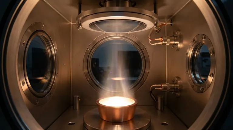
Step 3: Deposition (The Main Event)
This is where the film is actually formed. The target material is transported to the substrate within a controlled medium, most commonly a vacuum. Common deposition techniques include Physical Vapor Deposition (PVD) and Chemical Vapor Deposition (CVD), each offering different levels of control over the film's structure.
Step 4: Post-Deposition Treatment (Refinement)
Optionally, the newly formed film may undergo heat treatment, a process known as annealing. This step can help improve the film's crystal structure, relieve internal stresses, and enhance its adhesion to the substrate, effectively refining its properties.
Step 5: Analysis and Verification
Finally, the film is analyzed to ensure it meets specifications. A key parameter is thickness, often measured in nanometers, which can be determined by analyzing how light reflects and interferes between the film's top and bottom surfaces. This feedback loop allows engineers to modify the process for future depositions if needed.
What Defines a "Good" Thin Film?
The quality of a thin film is not an absolute measure but is defined by its suitability for a specific application. Several interdependent factors determine its final characteristics.
The Influence of the Substrate
The substrate is not a passive carrier. Its underlying material properties can profoundly impact the film, influencing everything from the film's crystalline orientation to its internal stress levels.
The Critical Role of Thickness
A thin film's properties can change dramatically with its thickness. Ranging from a few nanometers to several micrometers, thickness is a primary design parameter that governs optical, electrical, and mechanical behavior.
The Atomic-Level Actions
At the most fundamental level, film growth is governed by three phenomena: adsorption (atoms sticking to the surface), desorption (atoms leaving the surface), and surface diffusion (atoms moving around on the surface to find a stable position). The balance between these actions determines the film's density and structure.
The Impact of Deposition Method
The chosen deposition technique (like PVD or CVD) directly controls the energy and arrival rate of atoms hitting the substrate. This, in turn, dictates the film's final microstructure, density, and stress, tailoring it for specific performance requirements.
Understanding the Trade-offs
Choosing a thin film process is rarely about finding a single "best" method. It is an exercise in balancing competing technical and economic priorities.
Deposition Rate vs. Film Quality
Generally, depositing a film more slowly allows atoms more time for surface diffusion, resulting in a denser, more uniform, and higher-quality structure. Faster deposition rates increase throughput but can lead to more defects and lower-density films.
Process Control vs. Cost
Techniques that offer extremely precise control over factors like film thickness, composition, and structure are almost always more complex and expensive. The challenge is to match the level of process control to the actual performance requirements of the application without over-engineering.
Material and Substrate Compatibility
Not every material can be effectively deposited on any substrate. Chemical reactivity, differences in thermal expansion, and poor atomic-level adhesion can all lead to film failure. Significant engineering effort goes into finding compatible pairs of materials and processes.
Making the Right Choice for Your Application
Your final process selection must be guided by the primary goal of your component.
- If your primary focus is optical performance (e.g., anti-reflection coatings): Precision in film thickness and control over the material's refractive index are the most critical factors.
- If your primary focus is electronics (e.g., semiconductor layers): The absolute purity of the source material and the structural integrity of the resulting film are non-negotiable.
- If your primary focus is mechanical durability (e.g., hard coatings): Strong adhesion to the substrate and achieving a dense, low-stress film structure are paramount.
Ultimately, successful thin film fabrication is about mastering the relationship between your process variables and the final film properties you need to achieve.
Summary Table:
| Step | Key Action | Purpose |
|---|---|---|
| 1 | Source Material Selection | Choose the pure target material for the desired film function. |
| 2 | Substrate Preparation | Clean and prepare the base surface to ensure defect-free deposition. |
| 3 | Deposition (PVD/CVD) | Transport material to the substrate in a controlled environment (e.g., vacuum). |
| 4 | Post-Deposition Treatment | Anneal the film to refine structure, relieve stress, and improve adhesion. |
| 5 | Analysis & Verification | Measure thickness and properties to ensure they meet specifications. |
Ready to achieve precise, high-performance thin films for your lab? KINTEK specializes in lab equipment and consumables for thin film deposition, serving researchers and engineers in need of reliable PVD, CVD, and analysis solutions. Let us help you optimize your process for superior optical, electronic, or mechanical coatings. Contact our experts today to discuss your specific application requirements!
Visual Guide

Related Products
- Vacuum Hot Press Furnace Machine for Lamination and Heating
- Electron Beam Evaporation Coating Oxygen-Free Copper Crucible and Evaporation Boat
- Molybdenum Tungsten Tantalum Evaporation Boat for High Temperature Applications
- Lab Plastic PVC Calender Stretch Film Casting Machine for Film Testing
- Lab Blown Film Extrusion Three Layer Co-Extrusion Film Blowing Machine
People Also Ask
- What are the advantages of a vacuum hot press furnace for W-50%Cu? Achieve 99.6% Density at Lower Temperatures
- What advantages does a vacuum hot press furnace provide for LSLBO ceramic electrolytes? Achieve 94% Relative Density
- What role does the high vacuum environment play in sintering graphite film/aluminum composites? Optimize Your Bonding
- What role does mechanical pressure play during the vacuum diffusion bonding of tungsten and copper? Keys to Solid Bonding
- How does a vacuum hot press furnace contribute to the molding process of UHMWPE/nano-HAP composites?


