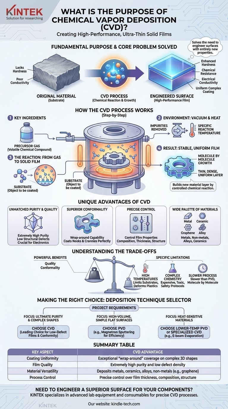
The fundamental purpose of Chemical Vapor Deposition (CVD) is to create a high-performance, ultra-thin solid film on the surface of a material, known as a substrate. It is not simply a coating process; it is a method of growing a new material layer by introducing a precursor gas into a heated, vacuum-sealed chamber, where a chemical reaction causes the gas to decompose and bond directly to the substrate, building the film one molecule at a time.
The core problem that CVD solves is the need to engineer a surface with entirely new properties—such as enhanced hardness, chemical resistance, or electrical conductivity—that the original material lacks. It achieves this with exceptional purity and the unique ability to uniformly coat complex, three-dimensional shapes.
How the CVD Process Fundamentally Works
To understand the purpose of CVD, it is essential to grasp its core mechanism. The process relies on a controlled chemical reaction rather than a physical application of material.
The Key Ingredients: Precursor and Substrate
The process begins with a precursor, which is a volatile chemical compound in gas form containing the elements you wish to deposit. This gas is injected into a chamber containing the object to be coated, known as the substrate.
The Environment: Vacuum and Heat
The entire process occurs under a vacuum. This is critical for removing impurities and allowing the precursor gas molecules to travel to the substrate surface without interference. The chamber is then heated to a specific reaction temperature.
The Reaction: From Gas to Solid Film
This heat provides the energy needed to break down the precursor gas molecules. The desired atoms or molecules then bond to the substrate's surface, forming a stable, solid film. Over time, this process builds up a thin, dense, and highly uniform layer across the entire exposed surface.
The Unique Advantages of CVD
CVD is chosen over other deposition methods when certain characteristics are non-negotiable for the final product.
Unmatched Purity and Quality
Because the process occurs in a vacuum and is built from a chemical reaction, the resulting films have extremely high purity and a very low count of structural defects. This is crucial for applications like high-performance electronics where even tiny impurities can cause failure.
Superior Conformality on Complex Shapes
One of CVD's most significant advantages is its "wrap-around" capability. Since the precursor is a gas, it naturally flows to cover every exposed nook and cranny of a complex or irregularly shaped component, resulting in a perfectly even coating.
Precise Control Over Film Properties
By carefully adjusting parameters like temperature, pressure, and gas composition, engineers can precisely control the final film's properties. This includes its chemical composition, thickness, crystal structure, and grain size.
A Wide Palette of Materials
The CVD process is incredibly versatile. It can be used to deposit a wide range of materials, including pure metals, non-metal films like graphene, multi-component alloys, and extremely hard ceramic or compound layers.
Understanding the Trade-offs
While powerful, CVD is not the universal solution for every application. Its process characteristics introduce specific limitations.
High Temperatures Can Limit Substrates
Traditional CVD often requires very high temperatures to initiate the chemical reaction. This can damage or deform substrates that are not thermally stable, such as certain plastics or sensitive electronic components.
Precursor Chemistry Can Be Complex
The precursor gases used in CVD can be expensive, toxic, or difficult to handle safely, requiring specialized equipment and safety protocols. The chemistry must be perfectly matched to the desired film and substrate.
It May Not Be the Fastest Method
Compared to some Physical Vapor Deposition (PVD) techniques, CVD can be a slower process. The film grows deliberately, molecule by molecule, which is excellent for quality but can be a bottleneck in high-volume manufacturing.
Making the Right Choice for Your Goal
Selecting a deposition technique depends entirely on the specific requirements of your project. CVD excels where quality and conformity are paramount.
- If your primary focus is ultimate purity and coating complex shapes: CVD is the leading choice due to its gas-phase nature and ability to produce low-defect films.
- If your primary focus is high-volume production on simple, flat surfaces: A PVD method like magnetron sputtering might be a more efficient and cost-effective solution.
- If your primary focus is coating heat-sensitive materials: You would need to consider a lower-temperature PVD process like e-beam evaporation or a specialized variant of CVD designed to operate at lower temperatures.
Ultimately, Chemical Vapor Deposition is the definitive tool for fundamentally transforming a material's surface into something more capable.
Summary Table:
| Key Aspect | CVD Advantage |
|---|---|
| Coating Uniformity | Exceptional "wrap-around" coverage on complex 3D shapes |
| Film Quality | Extremely high purity and low defect density |
| Material Versatility | Deposits metals, ceramics, alloys, and non-metals like graphene |
| Process Control | Precise control over film thickness, composition, and structure |
Need to engineer a superior surface for your components?
Chemical Vapor Deposition is the definitive solution for creating high-performance, ultra-thin films on complex geometries. KINTEK specializes in providing the advanced lab equipment and consumables necessary for precise CVD processes.
Contact our experts today to discuss how our solutions can help you achieve unparalleled purity, conformity, and control in your material coatings.
Visual Guide
Related Products
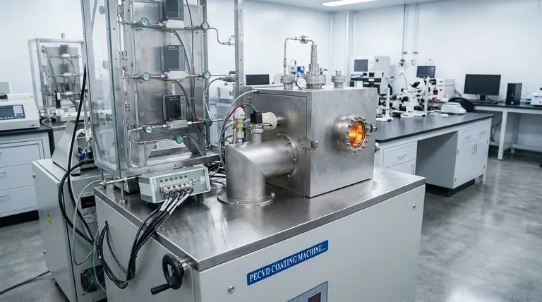
- Chemical Vapor Deposition CVD Equipment System Chamber Slide PECVD Tube Furnace with Liquid Gasifier PECVD Machine
- RF PECVD System Radio Frequency Plasma-Enhanced Chemical Vapor Deposition RF PECVD
- 915MHz MPCVD Diamond Machine Microwave Plasma Chemical Vapor Deposition System Reactor
- Customer Made Versatile CVD Tube Furnace Chemical Vapor Deposition Chamber System Equipment
- Microwave Plasma Chemical Vapor Deposition MPCVD Machine System Reactor for Lab and Diamond Growth
People Also Ask
- What are the advantages of chemical vapor deposition? Achieve Superior Thin Films for Your Lab
- What are the processes of vapor phase deposition? Understand CVD vs. PVD for Superior Thin Films
- Why is Chemical Vapor Deposition (CVD) equipment uniquely suited for constructing hierarchical superhydrophobic structures?
- What are the core advantages of PE-CVD in OLED encapsulation? Protect Sensitive Layers with Low-Temp Film Deposition
- What types of substrates are used in CVD to facilitate graphene films? Optimize Graphene Growth with the Right Catalyst


