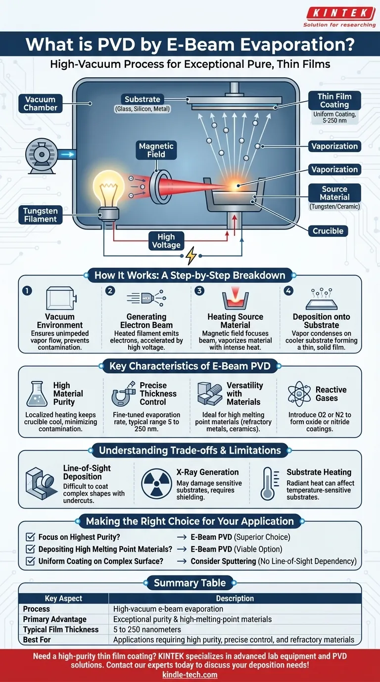
In short, Physical Vapor Deposition (PVD) by electron beam (e-beam) evaporation is a high-vacuum process used to create exceptionally pure, thin films. It works by firing a focused beam of high-energy electrons at a source material, causing it to vaporize. This vapor then travels through the vacuum and condenses onto a cooler substrate, forming a uniform coating.
The core principle of e-beam evaporation is using a precisely controlled electron beam as a heat source. This allows for the vaporization of a wide range of materials, including those with very high melting points, while minimizing contamination to produce coatings of superior purity.
How E-Beam Evaporation Works: A Step-by-Step Breakdown
To understand why this method is chosen for demanding applications, we must examine the mechanics of the process, which takes place entirely within a high-vacuum chamber.
The Vacuum Environment
The entire process occurs under high vacuum to ensure the evaporated material can travel to the substrate unimpeded. This near-empty environment prevents vapor atoms from colliding with air molecules, which would otherwise scatter them and introduce impurities into the film.
Generating the Electron Beam
A tungsten filament is heated by an electrical current, causing it to emit electrons. A high-voltage field then accelerates these electrons toward the source material at very high speeds.
Heating the Source Material
A magnetic field is used to bend the path of the electrons and focus them into a tight beam aimed at the source material, which is held in a crucible. The kinetic energy of the electrons is converted into intense thermal energy upon impact, heating the material to its evaporation or sublimation point.
Deposition onto the Substrate
The vaporized material travels in a straight line upward from the source. It then comes into contact with the cooler substrate (such as glass, silicon, or metal) positioned above, where it condenses and forms a thin, solid film.
Key Characteristics of E-Beam PVD
Engineers and scientists choose e-beam evaporation over other PVD methods like sputtering or thermal evaporation for several distinct advantages.
High Material Purity
The electron beam delivers highly localized heating directly to the source material. This means the surrounding crucible stays relatively cool, preventing it from melting or reacting with the source and contaminating the resulting film.
Precise Control Over Film Thickness
The rate of evaporation can be finely tuned by adjusting the electron beam's current, allowing for excellent control over the final film thickness. Coatings are typically in the range of 5 to 250 nanometers.
Versatility with Materials
Because the electron beam can generate extremely high temperatures, e-beam PVD is ideal for materials with very high melting points, such as refractory metals (e.g., tungsten, tantalum) and ceramics that are difficult or impossible to evaporate by other thermal methods.
The Role of Reactive Gases
To create non-metallic films, a reactive gas like oxygen or nitrogen can be introduced into the vacuum chamber during deposition. This allows the evaporated metal to react with the gas as it deposits, forming oxide or nitride coatings.
Understanding the Trade-offs and Limitations
No process is perfect. To make an informed decision, you must be aware of the inherent limitations of e-beam PVD.
Line-of-Sight Deposition
The vaporized material travels in a straight line from the source to the substrate. This makes it difficult to achieve uniform coatings on complex, three-dimensional objects with shadowed areas or undercuts.
X-Ray Generation
The impact of high-energy electrons can generate X-rays, which may damage sensitive substrates like certain electronic components or polymers. Proper shielding and process control are necessary to mitigate this risk.
Substrate Heating
A significant amount of energy is transferred to the substrate during the condensation process. This radiant heat can be problematic for temperature-sensitive substrates, potentially causing them to warp or degrade.
Making the Right Choice for Your Application
Selecting a deposition method depends entirely on the priorities of your project. E-beam evaporation excels in specific scenarios.
- If your primary focus is achieving the highest possible film purity: E-beam PVD is the superior choice due to its localized heating that minimizes crucible contamination.
- If your primary focus is depositing materials with extremely high melting points: The intense, focused energy of the electron beam makes it one of the few viable options.
- If your primary focus is uniformly coating a complex, non-flat surface: You should consider alternative methods like sputtering, which does not have the same line-of-sight dependency.
Ultimately, e-beam PVD is a powerful tool for creating high-performance thin films when purity and material choice are your most critical constraints.
Summary Table:
| Key Aspect | Description |
|---|---|
| Process | High-vacuum deposition using an electron beam to vaporize a source material. |
| Primary Advantage | Exceptional film purity and ability to coat high-melting-point materials. |
| Typical Film Thickness | 5 to 250 nanometers. |
| Best For | Applications requiring high purity, precise thickness control, and refractory materials. |
Need a high-purity thin film coating for your project?
KINTEK specializes in advanced lab equipment and consumables for precise PVD processes like e-beam evaporation. Whether you're developing semiconductors, optical coatings, or specialized sensors, our expertise and solutions can help you achieve superior film quality and performance.
Contact our experts today to discuss how we can support your laboratory's specific deposition needs!
Visual Guide
Related Products
- RF PECVD System Radio Frequency Plasma-Enhanced Chemical Vapor Deposition RF PECVD
- Molybdenum Tungsten Tantalum Evaporation Boat for High Temperature Applications
- Electron Beam Evaporation Coating Conductive Boron Nitride Crucible BN Crucible
- Chemical Vapor Deposition CVD Equipment System Chamber Slide PECVD Tube Furnace with Liquid Gasifier PECVD Machine
- E Beam Crucibles Electron Gun Beam Crucible for Evaporation
People Also Ask
- What are the advantages of PECVD? Enable Low-Temperature, High-Quality Thin-Film Deposition
- What is plasma activated chemical vapour deposition method? A Low-Temperature Solution for Advanced Coatings
- Why is PECVD environment friendly? Understanding the Eco-Friendly Benefits of Plasma-Enhanced Coating
- What is the principle of plasma enhanced chemical vapor deposition? Achieve Low-Temperature Thin Film Deposition
- Why does PECVD commonly use RF power input? For Precise Low-Temperature Thin Film Deposition