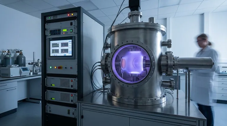
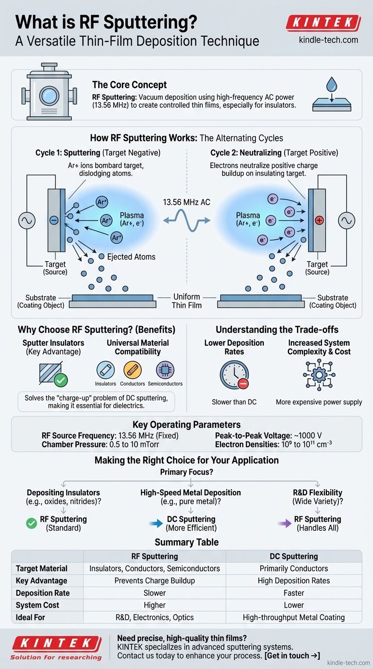
RF sputtering is a vacuum deposition technique used to create highly controlled thin films of material onto a surface. It uses a high-frequency alternating current (AC) power source to generate a plasma and bombard a source material, dislodging atoms that then coat a substrate. Its primary advantage is its ability to deposit insulating, or dielectric, materials.
The core problem RF sputtering solves is the inability of simpler DC sputtering methods to handle electrically insulating materials. By using an alternating electric field, RF sputtering prevents a disruptive charge buildup on the target, making it a versatile and essential tool for modern electronics and optics.
How RF Sputtering Works: The Core Mechanism
To understand RF sputtering, it's best to visualize the process step-by-step inside its vacuum chamber.
The Setup: Chamber, Gas, and Target
The entire process occurs in a vacuum chamber pumped down to a very low pressure. This chamber is then backfilled with a small, controlled amount of an inert gas, almost always Argon (Ar).
Inside, a target (the source material to be deposited) is positioned opposite a substrate (the object to be coated).
Igniting the Plasma with Radio Frequency
An AC power source, operating at a federally mandated radio frequency of 13.56 MHz, is applied to the target. This high-frequency electric field energizes the argon gas, stripping electrons from the argon atoms and creating a glowing, ionized gas known as a plasma.
This plasma is a mix of positive argon ions (Ar+) and free electrons.
The Alternating Cycles: Sputter and Neutralize
The use of an AC power source is what defines RF sputtering. The electric field rapidly oscillates, creating two distinct, repeating half-cycles.
-
The Sputtering Cycle (Target is Negative): In this brief phase, the target becomes negatively charged. This powerful negative potential attracts the positive argon ions from the plasma, which accelerate and slam into the target with significant kinetic energy. This bombardment physically knocks atoms loose from the target material.
-
The Neutralizing Cycle (Target is Positive): In the next phase, the target's polarity flips to positive. This attracts a shower of free electrons from the plasma. This is the crucial step for insulating targets, as these electrons neutralize the positive charge that would otherwise accumulate on the surface and stop the process.
Deposition on the Substrate
The atoms ejected from the target travel through the low-pressure chamber and land on the substrate. Over time, these atoms build up, nucleate, and grow into a uniform, high-purity thin film.
Why Choose RF Sputtering?
The key advantage of RF sputtering lies in its material versatility, which directly solves the primary limitation of its predecessor, DC sputtering.
The Unmatched Ability to Sputter Insulators
DC sputtering only works with electrically conductive targets. If you try to sputter an insulator (like silicon dioxide or aluminum oxide) with DC power, positive ions build up on the target's surface.
This phenomenon, called "charge-up," quickly repels further positive argon ions, effectively extinguishing the plasma and halting the sputtering process. RF sputtering's alternating field completely prevents this, making it the standard method for depositing dielectric films.
Universal Material Compatibility
Because the RF method works for insulators, it is also perfectly capable of depositing conductive and semiconductive materials. This makes it a highly flexible tool for research and development where many different types of materials may be used.
Understanding the Trade-offs
While powerful, RF sputtering is not always the optimal choice. It comes with clear performance and cost considerations.
Lower Deposition Rates
A significant drawback of RF sputtering is that it is generally slower than DC sputtering. The sputtering only occurs during the negative half-cycle, and the overall power transfer to the plasma can be less efficient. This makes it less ideal for high-throughput industrial applications involving conductive materials.
Increased System Complexity and Cost
An RF power system, which includes a high-frequency power supply and an impedance matching network, is significantly more complex and expensive than a simple DC power supply. This added cost can be a factor, especially when designing systems for coating very large substrates.
Key Operating Parameters
A typical RF sputtering process operates within a well-defined range of conditions:
- RF Source Frequency: 13.56 MHz (fixed)
- Chamber Pressure: 0.5 to 10 mTorr
- Peak-to-Peak Voltage: ~1000 V
- Electron Densities: 10⁹ to 10¹¹ cm⁻³
Making the Right Choice for Your Application
Selecting the correct sputtering technique depends entirely on your material and production goals.
- If your primary focus is depositing an insulating material (e.g., an oxide or nitride): RF sputtering is the necessary and standard industry choice.
- If your primary focus is high-speed, low-cost deposition of a conductive material (e.g., a pure metal): DC sputtering is almost always the more efficient and economical option.
- If your primary focus is research and development with a wide variety of materials: RF sputtering offers the greatest flexibility to handle conductors, semiconductors, and insulators with a single system.
Ultimately, RF sputtering's ability to manipulate non-conductive materials at the atomic level makes it a cornerstone technology for fabricating advanced microelectronics, optical coatings, and functional surfaces.
Summary Table:
| Aspect | RF Sputtering | DC Sputtering |
|---|---|---|
| Target Material | Insulators, Conductors, Semiconductors | Primarily Conductors |
| Key Advantage | Prevents charge buildup on insulating targets | High deposition rates for metals |
| Deposition Rate | Slower | Faster |
| System Cost | Higher (complex power supply) | Lower |
| Ideal For | R&D, Electronics, Optics | High-throughput metal coating |
Need to deposit precise, high-quality thin films for your research or production?
KINTEK specializes in providing advanced lab equipment, including sputtering systems, to meet the demanding needs of modern laboratories. Whether you are working with insulating, conductive, or semiconductive materials, our expertise can help you achieve superior results.
Contact us today to discuss how our solutions can enhance your thin-film deposition process and drive your innovations forward. Get in touch →
Visual Guide
Related Products
- RF PECVD System Radio Frequency Plasma-Enhanced Chemical Vapor Deposition RF PECVD
- Spark Plasma Sintering Furnace SPS Furnace
- Horizontal High Temperature Graphite Vacuum Graphitization Furnace
People Also Ask
- What is plasma enhanced chemical Vapour deposition process used for fabrication of? A Guide to Low-Temperature Thin Films
- How does plasma enhance CVD? Unlock Low-Temperature, High-Quality Film Deposition
- How does Radio Frequency Enhanced Plasma Chemical Vapour Deposition (RF-PECVD) work? Learn the Core Principles
- What is an example of PECVD? RF-PECVD for High-Quality Thin Film Deposition
- Why is a Matching Network Indispensable in RF-PECVD for Siloxane Films? Ensure Stable Plasma and Uniform Deposition


