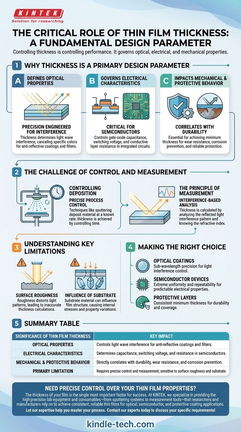
In short, the thickness of a thin film is one of its most critical design parameters. This single dimension, often measured in nanometers, directly dictates the film's physical properties and, therefore, its ultimate function. Whether for an anti-reflective lens coating, a semiconductor chip, or a solar panel, controlling the thickness is equivalent to controlling the performance of the final product.
The core significance of a thin film's thickness is that it is not merely a geometric measurement; it is a fundamental property that governs the film's interaction with light, electricity, and its environment. Mastering thickness is mastering the device's function.
Why Thickness Is a Primary Design Parameter
The properties of a finished thin film are determined by the substrate material, the deposition technique used, and, most importantly, the film's final thickness. Even a variation of a few nanometers can dramatically alter the outcome.
It Defines Optical Properties
Many optical applications, like lens coatings, rely on the principle of light wave interference.
The thickness of the film is precisely engineered to be a fraction of a light's wavelength. This causes light waves reflecting off the top and bottom surfaces of the film to interfere with each other, canceling out specific colors and reducing reflection.
It Governs Electrical Characteristics
In semiconductor manufacturing, thin films are everything. The thickness of a gate oxide layer in a transistor, for example, directly controls its capacitance and the voltage needed to switch it on or off.
Similarly, the thickness of conductive layers determines their electrical resistance, a critical factor for the efficiency and speed of an integrated circuit.
It Impacts Mechanical and Protective Behavior
For applications like protective barriers on tools or medical implants, thickness directly correlates with durability, wear resistance, and the ability to prevent corrosion.
Achieving a specific minimum thickness with uniform coverage is essential to ensure the film performs its protective function reliably over the product's lifespan.
The Challenge of Control and Measurement
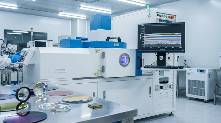
Because thickness is so critical, the processes for creating and measuring it must be exceptionally precise. Deposition techniques are controlled to create films ranging from a few angstroms (tenths of a nanometer) to many microns.
Controlling Deposition
Processes like sputtering involve depositing material at a known, constant rate. The desired thickness is achieved simply by running the process for a precise amount of time before cutting power to the source.
This level of control is fundamental to achieving repeatable results in high-volume manufacturing.
The Principle of Measurement
Thickness is often verified by analyzing the light interference pattern reflected from the film. By observing the peaks and valleys in the light spectrum, and knowing the material's refractive index, engineers can calculate the thickness with high accuracy.
This non-destructive method provides the crucial feedback needed to ensure the deposition process is performing as expected.
Understanding Key Limitations
While the goal is perfect control, real-world factors introduce complexity and potential for error. Understanding these trade-offs is key to successful application.
The Impact of Surface Roughness
The interference-based measurement technique relies on smooth, uniform surfaces to work correctly.
If the surface of the film or the underlying substrate is rough, it can distort the reflected light pattern. This distortion leads to inaccurate and unreliable thickness calculations, making process control difficult.
The Influence of the Substrate
A thin film's properties are not created in a vacuum. The underlying substrate material can influence how the film's atoms arrange themselves during deposition.
This can cause internal stresses or structural variations within the film that interact with its thickness, subtly changing its final characteristics.
Making the Right Choice for Your Goal
The level of precision required for film thickness depends entirely on the application.
- If your primary focus is optical coatings: Your top priority is achieving sub-wavelength precision to control light interference for specific colors.
- If your primary focus is semiconductor devices: You need extreme uniformity and repeatability to ensure predictable electrical properties across millions of transistors.
- If your primary focus is protective or barrier layers: Your goal is to achieve a minimum required thickness consistently for durability and coverage, where slight variations may be acceptable.
Ultimately, controlling a thin film's thickness is the primary lever you have to define and optimize its function.
Summary Table:
| Significance of Thin Film Thickness | Key Impact |
|---|---|
| Optical Properties | Controls light wave interference for anti-reflective coatings and filters. |
| Electrical Characteristics | Determines capacitance, switching voltage, and resistance in semiconductors. |
| Mechanical & Protective Behavior | Directly correlates with durability, wear resistance, and corrosion prevention. |
| Primary Limitation | Requires precise control and measurement; sensitive to surface roughness and substrate. |
Need precise control over your thin film properties? The thickness of your film is the single most important factor for success. At KINTEK, we specialize in providing the high-precision lab equipment and consumables—from sputtering systems to measurement tools—that researchers and manufacturers rely on to achieve consistent, reliable thin films for optical, semiconductor, and protective coating applications. Let our expertise help you master your process. Contact our experts today to discuss your specific requirements!
Visual Guide
Related Products
- Aluminum-Plastic Flexible Packaging Film for Lithium Battery Packaging
- Thin-Layer Spectral Electrolysis Electrochemical Cell
People Also Ask
- What is the difference between monolayer and multilayer film? Choose the Right Packaging for Your Product
- What are the properties of Aluminium (Al) relevant to its use in coatings? High Reflectivity & Conductivity Explored
- What is the thinnest coating? Unlocking Unique Properties at the Atomic Scale
- How to tell if a lithium-ion battery is bad? Spot the critical signs of failure before it's too late.
- What is the difference between single layer film and multi layer film? A Guide to Material Selection

