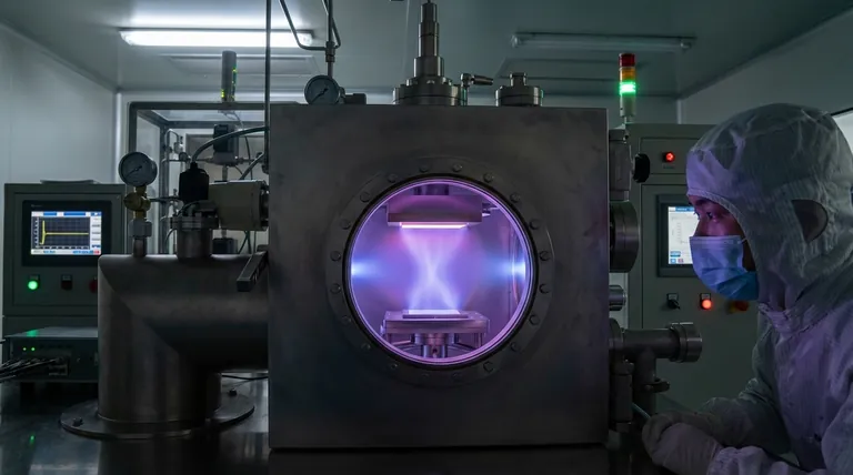
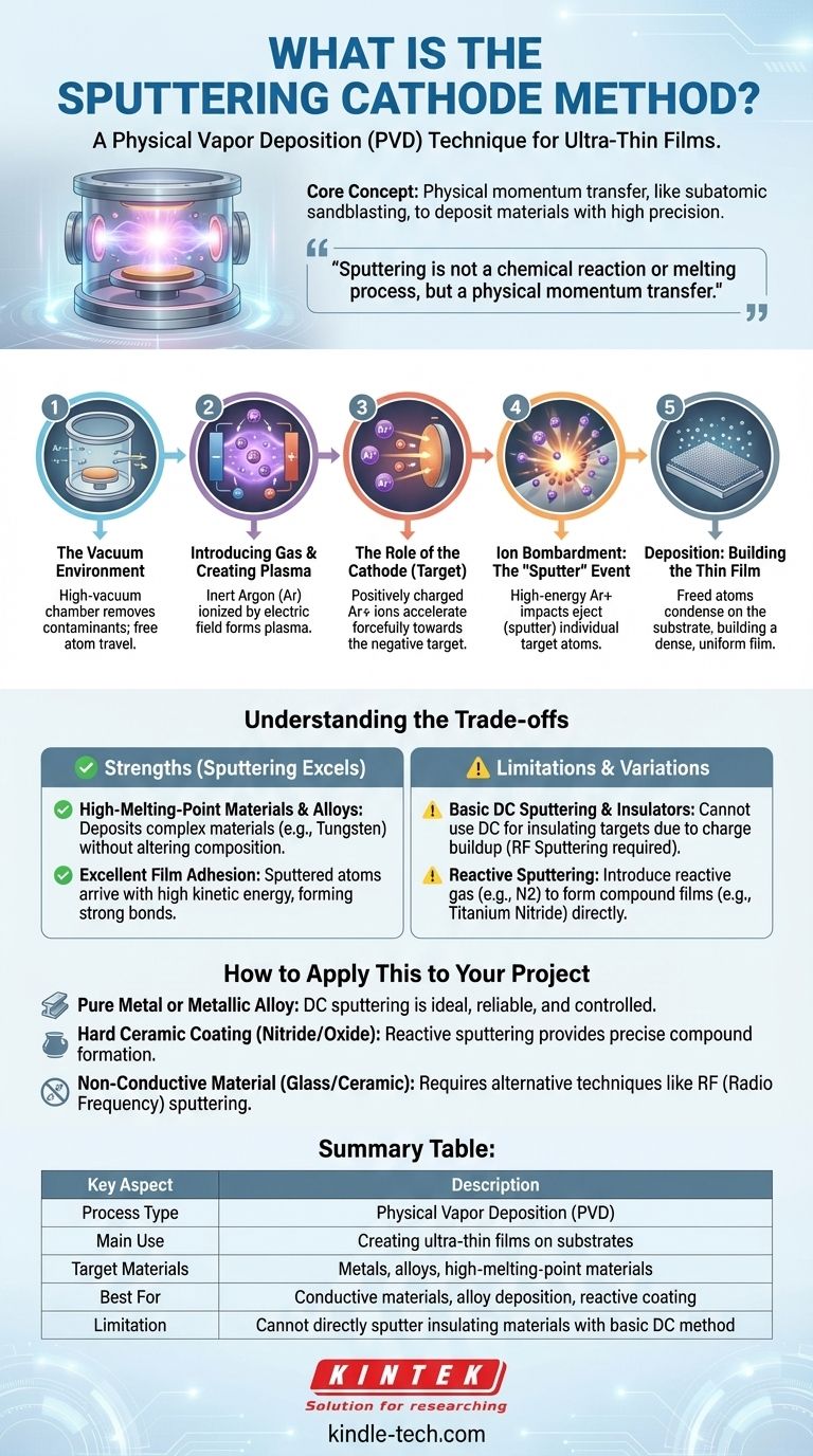
At its core, the sputtering cathode method is a physical vapor deposition (PVD) technique used to create ultra-thin films. The process involves placing a solid material, known as the target, into a vacuum chamber and bombarding it with high-energy ions from a plasma. These ion collisions are energetic enough to physically knock atoms off the target's surface, which then travel and condense onto a substrate, forming the desired thin film.
Sputtering is best understood not as a chemical reaction or a melting process, but as a physical momentum transfer. Think of it as a subatomic sandblasting, where individual atoms of a source material are dislodged by ion impacts and then re-deposited with high precision onto another surface.
How Sputtering Works: A Step-by-Step Breakdown
To truly grasp the sputtering method, it's essential to understand the controlled sequence of events that takes place inside the vacuum chamber.
The Vacuum Environment
First, a substrate (the object to be coated) and a target (the coating material) are placed in a high-vacuum chamber. This vacuum is critical for removing contaminants and ensuring the sputtered atoms can travel freely from the target to the substrate without unwanted collisions.
Introducing the Gas and Creating Plasma
A small, controlled amount of an inert gas, almost always Argon (Ar), is introduced into the chamber. A strong DC electric field is then applied, designating the target as the negative electrode (cathode) and the substrate as the positive electrode (anode). This field energizes the gas, stripping electrons from the argon atoms and creating a glowing, ionized gas known as a plasma.
The Role of the Cathode (The Target)
The plasma is now a high-energy soup of positive argon ions (Ar+) and free electrons. Because opposite charges attract, the positively charged Ar+ ions are forcefully accelerated towards the negatively charged target (cathode).
Ion Bombardment: The "Sputter" Event
These high-energy Ar+ ions collide with the surface of the target. The impact transfers kinetic energy from the ion to the target material, much like a cue ball striking a rack of billiard balls. This energy transfer is sufficient to eject, or "sputter," individual atoms from the target's surface.
Deposition: Building the Thin Film
The newly freed atoms from the target material travel through the vacuum chamber and land on the surface of the substrate. As more and more atoms arrive, they condense and build upon one another, forming a dense, uniform, and extremely thin film.
Understanding the Trade-offs
Sputtering is a powerful and versatile technique, but it's not universally applicable. Understanding its strengths and weaknesses is key to using it effectively.
Strength: High-Melting-Point Materials and Alloys
Sputtering excels where other methods, like thermal evaporation, fail. Because it is a physical and not a thermal process, it can easily deposit materials with extremely high melting points (e.g., tungsten, tantalum) and complex alloys without altering their composition.
Strength: Excellent Film Adhesion
The sputtered atoms arrive at the substrate with considerable kinetic energy, which helps them form a very dense and strongly bonded film. The process can also include a "cathodic cleaning" step, where the polarity is temporarily reversed to bombard the substrate with ions, cleaning its surface of contaminants and further improving film adhesion.
Limitation: Basic DC Sputtering and Insulators
The basic method described here, DC sputtering, works only for electrically conductive targets (metals). If the target is an insulator, the positive charge from the arriving Ar+ ions cannot dissipate. This charge buildup eventually repels further ions, stopping the sputtering process entirely. More advanced techniques, like RF sputtering, are required for insulating materials.
Variation: Reactive Sputtering
This limitation can be turned into an advantage. By introducing a reactive gas (like Nitrogen or Oxygen) along with the Argon, you can perform reactive sputtering. For example, by sputtering a titanium target in the presence of nitrogen gas, the sputtered titanium atoms react with the nitrogen to form a titanium nitride (TiN) film on the substrate—a hard, wear-resistant ceramic coating.
How to Apply This to Your Project
Choosing the right deposition method depends entirely on your material and your desired outcome.
- If your primary focus is depositing a pure metal or a metallic alloy: DC sputtering is an ideal, reliable, and highly controlled method, especially for materials that are difficult to melt.
- If your primary focus is creating a hard ceramic coating like a nitride or oxide: Reactive sputtering provides a precise way to form these compound films directly on your substrate.
- If your primary focus is coating a non-conductive material (like glass or a ceramic): Basic DC sputtering is not the right tool; you must investigate alternative techniques like RF (Radio Frequency) sputtering.
Ultimately, the sputtering cathode method provides an exceptional level of control for engineering surfaces at the atomic level.
Summary Table:
| Key Aspect | Description |
|---|---|
| Process Type | Physical Vapor Deposition (PVD) |
| Main Use | Creating ultra-thin films on substrates |
| Target Materials | Metals, alloys, high-melting-point materials |
| Best For | Conductive materials, alloy deposition, reactive coating |
| Limitation | Cannot directly sputter insulating materials with basic DC method |
Ready to enhance your thin film deposition capabilities? KINTEK specializes in laboratory sputtering equipment and consumables for research and industrial applications. Whether you're working with metals, alloys, or need reactive sputtering capabilities, our experts can help you select the right system for your specific needs. Contact us today to discuss how our sputtering solutions can advance your materials research and development projects!
Visual Guide
Related Products
- Reference Electrode Calomel Silver Chloride Mercury Sulfate for Laboratory Use
- Laboratory CVD Boron Doped Diamond Materials
- Chemical Vapor Deposition CVD Equipment System Chamber Slide PECVD Tube Furnace with Liquid Gasifier PECVD Machine
- Multifunctional Electrolytic Electrochemical Cell Water Bath Single Layer Double Layer
- Battery Lab Equipment 304 Stainless Steel Strip Foil 20um Thick for Battery Test
People Also Ask
- What is the recommended maintenance for the filling solution of a reference electrode? A Guide to Stable & Accurate Readings
- Why is the selection of a high-quality reference electrode critical in the electrochemical synthesis? | KINTEK
- What is the purpose of the reference electrode? Achieve Stable & Accurate Electrochemical Measurements
- Which electrode is used as a reference? A Guide to Accurate Electrochemical Measurements
- How does the selection of reference electrodes correlate with electrolyte pH in HER testing? Ensure Precise Potential