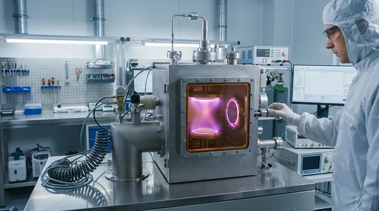
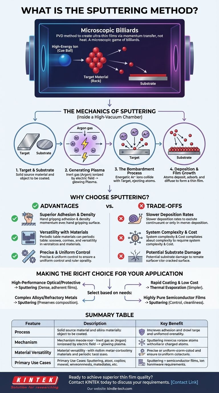
In essence, sputtering is a physical vapor deposition (PVD) method used to create ultra-thin films of material. The process works by ejecting atoms from a source material, known as a "target," by bombarding it with energized gaseous ions in a vacuum. These ejected atoms then travel and deposit onto a "substrate," gradually building up a thin, uniform film.
Sputtering is fundamentally a process of momentum transfer, not heat. Think of it as a microscopic game of billiards: a high-energy ion (the cue ball) strikes a target material (the rack of balls), knocking atoms loose that then coat a nearby surface. This physical impact mechanism is what gives sputtered films their unique and desirable properties.
The Mechanics of Sputtering
To understand sputtering, it’s helpful to break the process down into its core stages. The entire process takes place inside a high-vacuum chamber to ensure the purity of the film.
The Target and Substrate
The target is a solid slab of the material you wish to deposit as a thin film. This can be a pure metal, an alloy, or a ceramic compound. The substrate is the object you are coating, such as a silicon wafer, a piece of glass, or a medical implant.
Generating the Plasma
The process begins by introducing a small amount of an inert gas, typically Argon, into the vacuum chamber. An electric field is then applied, which ionizes the gas atoms, stripping them of electrons and creating a glowing, energized state of matter known as plasma.
The Bombardment Process
These newly formed, positively charged Argon ions are accelerated by the electric field and directed with great force toward the negatively charged target. When these ions collide with the target, their kinetic energy is transferred to the target atoms, physically knocking them loose from the source material.
Deposition and Film Growth
The ejected atoms travel through the vacuum chamber and land on the substrate. Upon arrival, they stick to the surface (adsorption) and arrange themselves (surface diffusion) to form a dense, thin, and highly adherent film. The process is continued until the desired film thickness is achieved.
Why Choose Sputtering? Key Advantages
Sputtering is chosen over other deposition methods for several critical reasons, primarily related to the quality and consistency of the final film.
Superior Adhesion and Density
Because sputtered atoms arrive at the substrate with significant kinetic energy, they embed themselves more firmly onto the surface. This results in films with excellent adhesion and a denser, less porous structure compared to methods like thermal evaporation.
Versatility with Materials
Sputtering can deposit a vast range of materials, including complex alloys, compounds, and high-melting-point refractory metals. Since it doesn't rely on melting the target, the composition of an alloy target is accurately replicated in the deposited film.
Precise and Uniform Control
The deposition rate in sputtering can be precisely controlled by managing the power and gas pressure. This allows for the creation of extremely uniform films over large substrate areas, a critical requirement in industries like semiconductor and display manufacturing.
Understanding the Trade-offs
No single method is perfect for every scenario. Sputtering has specific limitations that make other methods more suitable in certain contexts.
Slower Deposition Rates
Generally, sputtering is a slower process compared to high-rate thermal evaporation. For applications where film quality is secondary to production speed, sputtering may not be the most efficient choice.
System Complexity and Cost
A sputtering system requires a high-vacuum chamber, sophisticated power supplies, and gas flow controllers. This makes the equipment more complex and expensive than simpler techniques like spin coating or drop casting.
Potential Substrate Damage
The high-energy nature of the sputtering process can sometimes cause heating or even minor structural damage to very delicate substrates, such as certain polymers or biological samples.
Making the Right Choice for Your Application
Selecting the correct deposition method depends entirely on the material properties and performance you need to achieve.
- If your primary focus is high-performance optical coatings or durable protective layers: Sputtering is often the ideal choice due to the dense, well-adhered films it produces.
- If your primary focus is depositing complex alloys or refractory metals without altering their composition: Sputtering excels because its physical removal mechanism preserves the material's stoichiometry.
- If your primary focus is rapid coating and cost-effectiveness is paramount: A simpler method like thermal evaporation might be a more suitable choice for less demanding applications.
- If your primary focus is creating highly pure films for semiconductors: Sputtering provides the control and cleanliness required for advanced electronic devices.
By understanding this core mechanism of physical bombardment, you can strategically leverage sputtering to achieve superior film quality for your most demanding applications.
Summary Table:
| Feature | Description | Key Benefit |
|---|---|---|
| Process | Physical vapor deposition (PVD) via momentum transfer. | Does not rely on melting; preserves material composition. |
| Mechanism | Ejects target atoms using energized gas ions in a vacuum. | Creates dense, highly adherent films with excellent uniformity. |
| Material Versatility | Can deposit pure metals, alloys, and ceramics. | Ideal for complex materials and high-melting-point metals. |
| Primary Use Cases | Semiconductor manufacturing, optical coatings, durable protective layers. | Delivers the high-quality, consistent films required for advanced technology. |
Ready to achieve superior thin film quality for your lab?
Sputtering is essential for applications demanding high-performance optical coatings, durable protective layers, and precise semiconductor films. KINTEK specializes in providing the advanced lab equipment and consumables you need to leverage this powerful technology.
Our expertise ensures you get the right sputtering solutions for your specific materials and substrates, helping you create dense, uniform, and highly adherent films with confidence.
Contact KINTALK today to discuss your thin film deposition requirements and discover how our solutions can enhance your laboratory's capabilities.
Visual Guide
Related Products
- Spark Plasma Sintering Furnace SPS Furnace
- Vacuum Induction Melting Spinning System Arc Melting Furnace
- Chemical Vapor Deposition CVD Equipment System Chamber Slide PECVD Tube Furnace with Liquid Gasifier PECVD Machine
- Customer Made Versatile CVD Tube Furnace Chemical Vapor Deposition Chamber System Equipment
People Also Ask
- What are the advantages of CAMI/SPS for W-Cu composite preparation? Reduce cycles from hours to seconds.
- What is the process fundamentals of spark plasma sintering? Achieve Rapid, High-Density Material Consolidation
- What is the mechanism of SPS process? A Deep Dive into Rapid, Low-Temperature Sintering
- What are the fundamentals of spark plasma sintering process? Unlock Rapid, High-Performance Material Consolidation
- What is SPS sintering method? A Guide to High-Speed, High-Performance Material Fabrication


