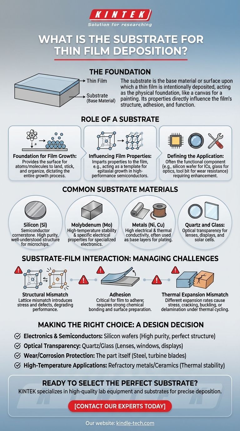
In thin film deposition, the substrate is the base material or surface upon which a thin film is intentionally deposited. It acts as the physical foundation for the film, much like a canvas for a painting. The choice of substrate is critical, as its properties directly influence the structure, adhesion, and ultimate function of the final coated product.
The substrate is far more than a passive holder; it is an active component in the deposition process. Its chemical and physical characteristics—from crystal structure to thermal expansion—are foundational to the quality and performance of the thin film itself.
What is the Role of a Substrate?
Understanding the substrate's function is key to understanding the entire deposition process. It serves several critical purposes beyond simply being a surface to coat.
The Foundation for Film Growth
The substrate provides the physical surface where atoms or molecules from the deposition source (e.g., a vapor in PVD or chemical precursors in CVD) land, stick, and organize. The initial interaction between the deposition material and the substrate surface dictates the entire growth process that follows.
Influencing Film Properties
The substrate’s properties are imparted to the film. For example, the crystalline structure of a substrate can act as a template, influencing the crystal orientation of the growing film. This is known as epitaxial growth and is crucial in the manufacturing of high-performance semiconductors.
Defining the Application
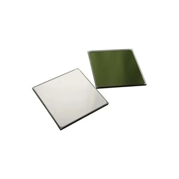
In many cases, the substrate is the functional component that requires enhancement. The thin film is simply the means of improving it. A silicon wafer is the substrate for building integrated circuits, a glass pane is the substrate for an anti-reflective coating, and a metal tool bit is the substrate for a wear-resistant coating.
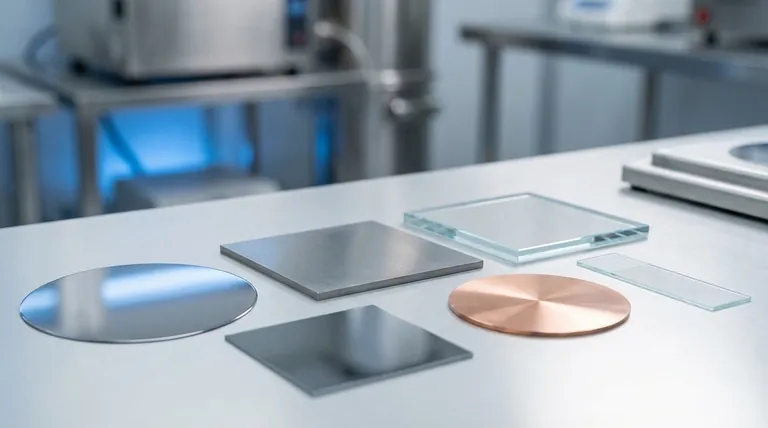
Common Substrate Materials
The choice of substrate is dictated entirely by the end-use application. While countless materials can be used, a few are particularly common in major industries.
Silicon (Si)
Silicon is the cornerstone of the semiconductor industry. As a substrate, its high purity, well-understood crystalline structure, and established manufacturing processes make it the default choice for creating microchips and other electronic components.
Molybdenum (Mo)
Molybdenum is often used in applications requiring stability at high temperatures or specific electronic properties. Its structural properties are a known factor in film growth, making it a well-characterized substrate for research and specialized electronics.
Metals (Ni, Cu)
Metals like nickel and copper are common substrates, particularly when the final product requires high electrical or thermal conductivity. They are also frequently used as a base layer for subsequent plating processes like electroplating.
Quartz and Glass
When optical transparency is the primary requirement, quartz and glass are the ideal substrates. They are used for everything from coated lenses and optical filters to transparent electrodes for displays and solar cells.
Understanding the Trade-offs: The Substrate-Film Interaction
The success of a thin film coating depends entirely on the compatibility between the film and the substrate. Several key challenges must be managed.
Structural Mismatch
A significant issue is the structural mismatch between the crystal lattice of the substrate and that of the film. The references note a mismatch of ~13% for molybdenum and ~20% for silicon with certain films. This mismatch introduces stress and defects into the film, which can degrade its electrical, optical, or mechanical performance.
Adhesion
A thin film is useless if it does not adhere properly to the substrate. Adhesion depends on the chemical bonding and physical forces between the two materials. The substrate surface must often be meticulously cleaned or treated to promote strong bonding and prevent the film from peeling or flaking off.
Thermal Expansion Mismatch
If the substrate and the thin film expand and contract at different rates with temperature changes, immense stress can build up. This mismatch can cause the film to crack, buckle, or delaminate, especially in applications that experience thermal cycling.
Making the Right Choice for Your Goal
Selecting a substrate is a critical design decision based on the intended outcome.
- If your primary focus is electronics and semiconductors: Silicon wafers are the industry standard due to their high purity and perfect crystalline structure.
- If your primary focus is optical transparency: Quartz or specialized glass is necessary for applications like lenses, windows, and displays.
- If your primary focus is wear resistance or corrosion protection: The substrate is often the part itself—a steel tool, a turbine blade, or a medical implant—chosen for its bulk mechanical properties.
- If your primary focus is high-temperature applications: Refractory metals like molybdenum or ceramic substrates are chosen for their ability to remain stable under extreme thermal stress.
Ultimately, the substrate is not an afterthought but a foundational element that defines the capabilities and reliability of the final product.
Summary Table:
| Common Substrate Material | Primary Application/Use Case |
|---|---|
| Silicon (Si) | Semiconductor and microelectronics |
| Molybdenum (Mo) | High-temperature and specialized electronics |
| Metals (Ni, Cu) | High conductivity and plating base layers |
| Quartz and Glass | Optical transparency (lenses, displays, solar cells) |
Ready to select the perfect substrate for your thin film application?
KINTEK specializes in providing high-quality lab equipment and consumables, including substrates tailored for precise deposition processes. Whether you're working with semiconductors, optics, or high-temperature materials, our expertise ensures your foundation is solid.
Contact our experts today to discuss your specific needs and discover how KINTEK can support your laboratory's success with reliable, performance-driven solutions.
Visual Guide
Related Products
- Aluminized Ceramic Evaporation Boat for Thin Film Deposition
- Tungsten Evaporation Boat for Thin Film Deposition
- Molybdenum Tungsten Tantalum Evaporation Boat for High Temperature Applications
- Electron Beam Evaporation Coating Oxygen-Free Copper Crucible and Evaporation Boat
- Hemispherical Bottom Tungsten Molybdenum Evaporation Boat
People Also Ask
- What is the chemical method for thin film deposition? Build Films from the Molecular Level Up
- What is the process of thin film in semiconductor? Build the Layers of Modern Electronics
- What are the applications of thin films deposition? Unlock New Possibilities for Your Materials
- What are the alternatives to sputtering? Choose the Right Thin Film Deposition Method
- What is the widely used boat made of in thermal evaporation? Choosing the Right Material for High-Purity Deposition