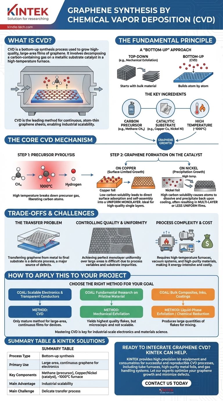
In essence, Chemical Vapor Deposition (CVD) is a synthesis process used to grow high-quality, large-area films of graphene. It functions by introducing a carbon-containing gas (a precursor) into a high-temperature furnace, where it decomposes on the surface of a metallic substrate, which acts as a catalyst. These decomposed carbon atoms then arrange themselves into the hexagonal lattice structure of graphene.
Chemical Vapor Deposition is the leading industrial method for producing graphene not as a powder, but as a continuous, atom-thin sheet. Its primary advantage is scalability, enabling the creation of films large enough for electronic applications, a feat unattainable with most other methods.
The Fundamental Principle: Building Graphene Atom by Atom
A "Bottom-Up" Approach
Graphene synthesis is broadly divided into two categories: "top-down" and "bottom-up."
Top-down methods, like mechanical exfoliation, start with a large piece of graphite and break it down into single layers. In contrast, CVD is a bottom-up method. It starts with individual carbon atoms from a gas and builds the graphene structure from scratch, similar to laying individual tiles to form a mosaic.
The Key Ingredients
The CVD process for graphene relies on three core components working in concert:
- Carbon Precursor: A hydrocarbon gas, most commonly methane (CH₄), that serves as the source of carbon atoms.
- Catalytic Substrate: A transition metal foil, typically Copper (Cu) or Nickel (Ni), on which the graphene grows. The metal's role is to dramatically lower the energy required for the reaction.
- High Temperature: The process occurs in a furnace at temperatures often approaching 1000°C to provide the energy needed to break down the precursor gas and facilitate atom arrangement.
The Core CVD Mechanism
The synthesis of graphene via CVD is a two-step process that occurs inside the reaction chamber.
Step 1: Precursor Pyrolysis
First, the high temperature causes the precursor gas to decompose. For example, methane breaks down into carbon and hydrogen atoms.
This step, known as pyrolysis, effectively liberates the individual carbon atoms that will be used to construct the graphene sheet.
Step 2: Graphene Formation on the Catalyst
Once free, the carbon atoms form the graphene lattice on the metal substrate. The exact mechanism depends heavily on the chosen metal.
On Copper, growth is a surface-limited process. Carbon has very low solubility in copper, so atoms adsorb directly onto the foil's surface and self-assemble into a single, uniform monolayer of graphene. This makes copper ideal for producing high-quality single-layer films.
On Nickel, the mechanism is different. Carbon has higher solubility in nickel, so atoms first dissolve into the bulk metal at high temperature. As the metal is cooled, the carbon's solubility decreases, forcing the dissolved atoms to precipitate back onto the surface, where they form graphene layers. This can result in multi-layer or less uniform films.
Understanding the Trade-offs and Challenges
While powerful, CVD is not without its complexities and limitations. Understanding these trade-offs is crucial for any practical application.
The Transfer Problem
Graphene grown via CVD is formed on a metal foil, but most electronic applications require it to be on an insulating substrate like silicon dioxide. This necessitates a transfer process.
The graphene film must be carefully lifted off the metal and moved to the final substrate. This delicate step is a primary source of defects, wrinkles, tears, and contamination that can degrade the graphene's exceptional properties.
Controlling Quality and Uniformity
Achieving a perfectly uniform, defect-free monolayer across a large area is extremely difficult.
Factors like gas flow, temperature gradients, and the purity of the metal foil can lead to the formation of multi-layer patches, grain boundaries (seams between different growing domains), and vacancies in the atomic lattice. The electrical properties of the film are highly dependent on this structural quality.
Process Complexity and Cost
CVD requires specialized equipment, including high-temperature furnaces, vacuum systems, and precise gas flow controllers. The need for high-purity metal foils and the energy-intensive nature of the process contribute to its overall cost and complexity.
How to Apply This to Your Project
The best synthesis method is entirely dependent on your end goal. CVD is a powerful tool, but it is not a universal solution.
- If your primary focus is scalable electronics or transparent conductors: CVD is the most viable path. It is the only mature method for producing the large-area, continuous graphene films required for devices like touch screens, sensors, and next-generation transistors.
- If your primary focus is fundamental research on pristine material: Mechanical exfoliation (the "Scotch tape method") is superior. It yields the highest-quality, most electronically perfect graphene flakes, but they are microscopic and not scalable.
- If your primary focus is bulk composites, inks, or coatings: Liquid-phase exfoliation or the chemical reduction of graphene oxide are better choices. These top-down methods produce large quantities of graphene flakes ideal for mixing into polymers, paints, or batteries.
Ultimately, mastering CVD is key to unlocking graphene's potential for transforming electronics and materials science on an industrial scale.
Summary Table:
| Aspect | Key Detail |
|---|---|
| Process Type | Bottom-up synthesis |
| Primary Use | Large-area, continuous graphene films for electronics |
| Key Components | Methane (precursor), Copper/Nickel (catalyst), ~1000°C furnace |
| Main Advantage | Industrial scalability |
| Main Challenge | Delicate transfer process to final substrates |
Ready to Integrate Graphene CVD into Your Lab Workflow?
Mastering the synthesis of high-quality graphene is crucial for next-generation electronics and materials science. KINTEK specializes in providing the high-precision lab equipment and consumables—from tube furnaces to high-purity metal foils and gas handling systems—that are essential for a successful and reproducible CVD process.
Let us help you achieve your research and development goals. Our experts can assist you in selecting the right tools to optimize your graphene growth, ensuring uniformity and minimizing defects.
Contact us today via our contact form to discuss your specific laboratory needs and how KINTEK can support your innovation in advanced materials.
Visual Guide
Related Products
- Custom CVD Diamond Coating for Lab Applications
- CVD Diamond for Thermal Management Applications
- Carbon Graphite Plate Manufactured by Isostatic Pressing Method
- Laboratory CVD Boron Doped Diamond Materials
- RF PECVD System Radio Frequency Plasma-Enhanced Chemical Vapor Deposition RF PECVD
People Also Ask
- What is CVD coated? A Guide to Superior Wear Resistance for Complex Parts
- What are the advantages of CVD coating? Superior Hardness and Uniformity for Demanding Applications
- What is the use of CVD coating? Enhance Durability and Functionality for Your Components
- Can you coat something in diamond? Unlock Unmatched Hardness and Thermal Conductivity
- What is CVD diamond coating? Grow a Super-Hard, High-Performance Diamond Layer