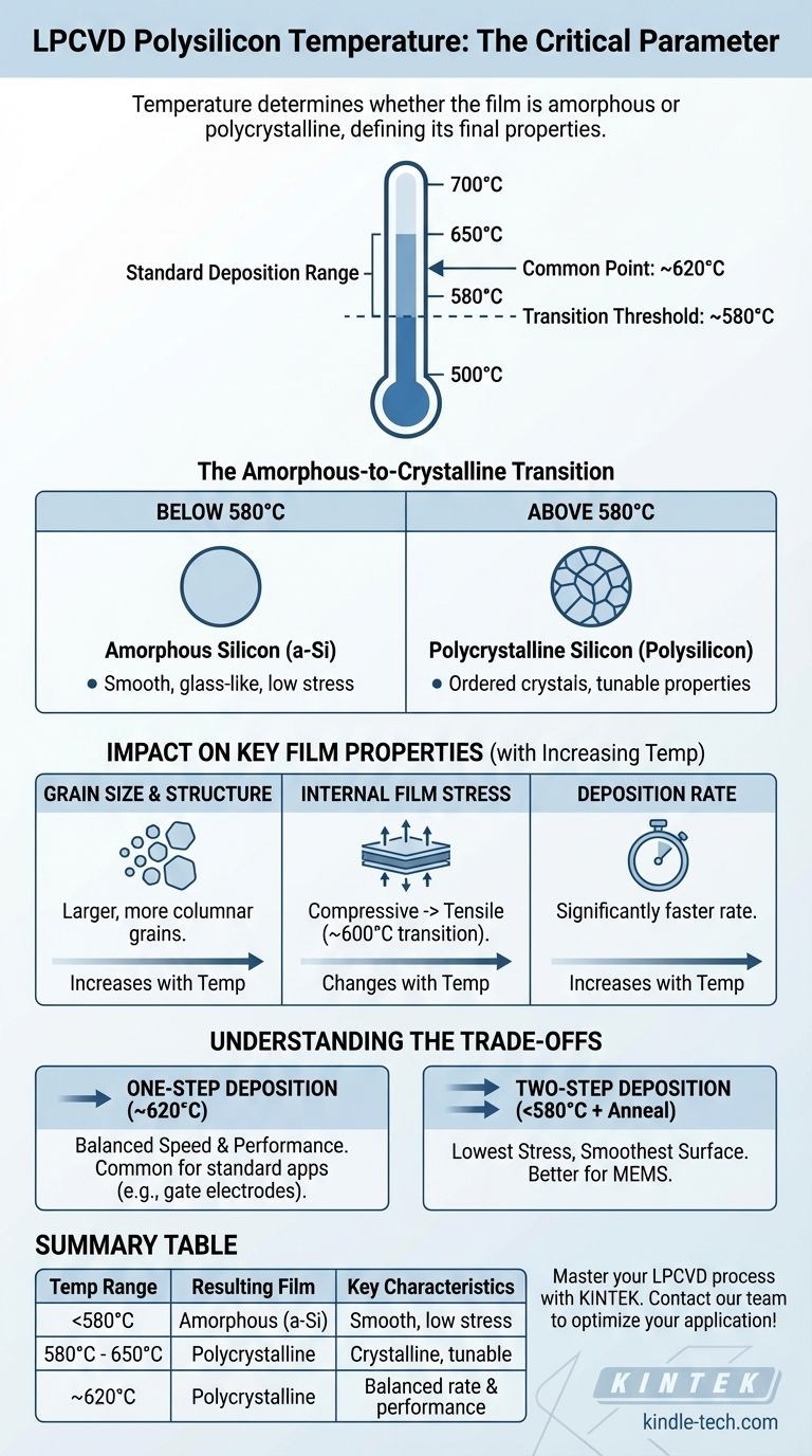
The standard deposition temperature for LPCVD polysilicon is not a single value but a critical range, typically between 580°C and 650°C. The most common temperature for depositing a polycrystalline film directly is approximately 620°C. This temperature is deliberately chosen to control the crystalline structure of the silicon film as it forms.
The specific temperature is the most important parameter in the process because it determines whether the silicon film is deposited in an amorphous state or a polycrystalline one. This choice fundamentally dictates the film's final grain structure, internal stress, and electrical characteristics.
Why Temperature is the Defining Process Parameter
The temperature inside the LPCVD (Low-Pressure Chemical Vapor Deposition) furnace directly controls the surface mobility of silicon atoms arriving from the source gas (typically silane, SiH₄). This mobility dictates how they arrange themselves, leading to vastly different materials.
The Amorphous-to-Crystalline Transition
There is a critical temperature threshold, generally around 580°C.
Below this temperature, atoms lack the energy to find an ordered crystal lattice site before being buried by subsequent atoms. The result is a smooth, glass-like amorphous silicon (a-Si) film.
Above this temperature, atoms have enough energy to move and form small, ordered crystalline structures known as grains. The result is a polycrystalline silicon (polysilicon) film.
Controlling Final Film Properties
The choice between depositing an amorphous or polycrystalline film is a deliberate engineering decision. A film deposited as amorphous and later crystallized with a high-temperature anneal will have very different properties than a film deposited directly as polysilicon.
Impact of Temperature on Key Film Properties
Varying the temperature within the deposition window allows engineers to fine-tune the material's characteristics for specific device applications.
Grain Size and Structure
As the deposition temperature increases from 580°C to 650°C, the resulting grain size generally becomes larger. The structure also changes, often transitioning from smaller, randomly oriented grains to larger, more columnar grains.
Internal Film Stress
Temperature has a profound effect on the residual stress of the film, which is critical for mechanical stability. There is often a stress transition point around 600°C, where the film's stress changes from compressive to tensile as the temperature rises.
Deposition Rate
The chemical reaction for depositing silicon is thermally activated. Therefore, a higher temperature results in a significantly faster deposition rate. This has direct implications for manufacturing throughput.
Understanding the Trade-offs
Selecting a deposition temperature involves balancing competing objectives. The "best" temperature is always a compromise based on the end goal.
Throughput vs. Film Quality
While a higher temperature (~650°C) increases deposition rate and thus throughput, it can also lead to larger grains and higher tensile stress. This may be unacceptable for certain applications, such as in Micro-Electro-Mechanical Systems (MEMS), where low stress is paramount.
One-Step vs. Two-Step Deposition
Depositing directly in the polycrystalline range (~620°C) is a simple, one-step process.
However, for applications demanding the lowest possible stress and smoothest surface, a two-step process is often superior. This involves depositing a perfectly smooth amorphous film at a lower temperature (<580°C) and then crystallizing it in a separate, controlled anneal step. This adds process time but yields a higher-quality film.
Selecting the Right Temperature for Your Application
The optimal temperature is dictated entirely by the requirements of the final device.
- If your primary focus is creating a low-stress, smooth film (e.g., for MEMS structures): Deposit in the amorphous regime (below 580°C) and follow with a separate crystallization anneal.
- If your primary focus is high-throughput manufacturing for standard applications (e.g., transistor gate electrodes): Deposit directly in the polycrystalline regime, typically around 620°C to 625°C, to balance speed and performance.
- If your primary focus is achieving a specific crystal texture or grain size: Meticulously control the temperature within the 580°C to 650°C window, as small variations have a significant impact on microstructure.
Ultimately, mastering the LPCVD polysilicon process begins with understanding that temperature is the fundamental lever for engineering the film's final properties.
Summary Table:
| Temperature Range | Resulting Film Structure | Key Characteristics |
|---|---|---|
| Below 580°C | Amorphous Silicon (a-Si) | Smooth, glass-like, low stress |
| 580°C - 650°C | Polycrystalline Silicon (Polysilicon) | Crystalline grains, tunable properties |
| ~620°C (Common) | Polycrystalline Silicon | Balanced deposition rate and performance |
Need precise control over your LPCVD polysilicon deposition? The temperature you choose is the single most important factor for your film's grain structure, stress, and electrical performance. KINTEK specializes in high-quality lab equipment and consumables for advanced semiconductor and MEMS processing. Our experts can help you select the right furnace and process parameters to achieve your specific film properties. Contact our team today to discuss your application requirements and optimize your LPCVD process!
Visual Guide
Related Products
- Inclined Rotary Plasma Enhanced Chemical Vapor Deposition PECVD Equipment Tube Furnace Machine
- Laboratory CVD Boron Doped Diamond Materials
- Inclined Rotary Plasma Enhanced Chemical Vapor Deposition PECVD Equipment Tube Furnace Machine
- Chemical Vapor Deposition CVD Equipment System Chamber Slide PECVD Tube Furnace with Liquid Gasifier PECVD Machine
- 915MHz MPCVD Diamond Machine Microwave Plasma Chemical Vapor Deposition System Reactor
People Also Ask
- What are the benefits of plasma enhanced CVD? Achieve High-Quality, Low-Temperature Film Deposition
- How does PECVD facilitate Ru-C nanocomposite films? Precision Low-Temperature Thin Film Synthesis
- How does plasma enhanced chemical vapor deposition work? Enable Low-Temperature Thin Film Deposition
- What is plasma enhanced chemical vapour deposition PECVD used for? Enable Low-Temp Thin Films for Electronics & Solar
- How does PECVD equipment facilitate the directional growth of carbon nanotubes? Achieve Precision Vertical Alignment


