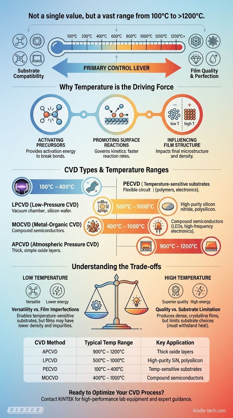
In short, the temperature for chemical vapor deposition (CVD) is not a single value but spans a vast range from as low as 100°C to over 1200°C. The precise temperature required depends entirely on the specific CVD technique being used, the precursor chemicals, and the desired properties of the final thin film.
The critical takeaway is that temperature is not merely a setting in CVD; it is the primary control lever. It dictates the reaction energy, deposition rate, and ultimate quality of the film, forcing a fundamental trade-off between film perfection and substrate compatibility.
Why Temperature is the Driving Force in CVD
To understand the different temperature ranges, you must first understand the role temperature plays. In CVD, heat is the energy source that drives the entire chemical process of converting gas-phase molecules into a solid-state thin film.
Activating Precursor Gases
The process begins with precursor gases, which contain the atoms needed for the film. Temperature provides the activation energy required to break the chemical bonds within these precursor molecules, making them reactive.
Without sufficient heat, the precursor gases will simply flow over the substrate without reacting, and no film will be deposited.
Promoting Surface Reactions
Once the precursors are broken down, the reactive species must adsorb onto the substrate surface, move around to find ideal lattice sites, and form stable chemical bonds. Temperature governs the speed of these surface reactions, a process known as kinetics.
Higher temperatures generally increase the reaction rate, leading to faster film growth.
Influencing Film Structure and Quality
Temperature has a profound impact on the final microstructure of the film.
High temperatures give surface atoms more energy to move around, allowing them to settle into a highly ordered, dense, and crystalline structure. Lower temperatures can "freeze" atoms in place before they find an ideal site, resulting in a disordered, less dense, or amorphous film.
Temperature Ranges by CVD Type
Because temperature is so fundamental, different CVD methods have been developed to operate within specific thermal regimes, each suited for different applications.
Atmospheric Pressure CVD (APCVD)
Typical Range: 900°C – 1200°C
This is a high-temperature process performed at ambient pressure. The high heat is necessary to achieve good reaction kinetics without the aid of a vacuum. It is often used for thick, simple oxide layers where substrate temperature tolerance is not a concern.
Low-Pressure CVD (LPCVD)
Typical Range: 500°C – 1000°C
By reducing the chamber pressure, the distance gas molecules can travel before colliding increases. This results in highly uniform films, even at slightly lower temperatures than APCVD. LPCVD is a workhorse for producing high-purity, high-quality films like silicon nitride and polysilicon in the semiconductor industry.
Plasma-Enhanced CVD (PECVD)
Typical Range: 100°C – 400°C
PECVD is the key low-temperature solution. Instead of relying solely on thermal energy, it uses an electromagnetic field (plasma) to energize the precursor gases and break them down.
This allows for deposition on temperature-sensitive substrates, such as polymers, plastics, or fully fabricated electronic devices that would be destroyed by the heat of LPCVD or APCVD.
Metal-Organic CVD (MOCVD)
Typical Range: 400°C – 1000°C
MOCVD is a highly versatile technique used for depositing complex materials, particularly compound semiconductors for LEDs and high-frequency electronics. It uses metal-organic precursors that can decompose across a wide temperature range, offering precise control over the film's composition and crystal structure.
Understanding the Trade-offs
Choosing a temperature is not about picking a number; it's about navigating a series of critical engineering trade-offs.
High Temperature: Quality vs. Substrate Limitation
High-temperature processes like LPCVD produce superior, dense, and highly crystalline films with low impurity levels. However, this thermal budget severely limits your choice of substrate. Any material that melts, warps, or degrades below the deposition temperature is incompatible.
Low Temperature: Versatility vs. Film Imperfections
Low-temperature processes like PECVD offer incredible versatility, enabling deposition on virtually any substrate. The trade-off is often in film quality. These films can have lower density, higher internal stress, and may incorporate impurities (like hydrogen from precursors) that can affect electrical or optical properties.
The Cost of Energy and Equipment
Achieving and maintaining high temperatures is energy-intensive and requires robust, expensive equipment like high-temperature furnaces and sophisticated cooling systems. Lower-temperature processes, while requiring complex plasma generators, can often have a lower overall energy cost.
Selecting the Right Process for Your Goal
Your choice of CVD method and its corresponding temperature range must be dictated by your final objective.
- If your primary focus is the highest possible crystalline quality and film purity: You will need to use a high-temperature process like LPCVD or MOCVD and select a substrate that can withstand the heat.
- If your primary focus is depositing on a temperature-sensitive substrate: A low-temperature method like PECVD is your essential, and often only, choice.
- If your primary focus is growing complex, epitaxial compound semiconductors: A specialized technique like MOCVD provides the necessary control over composition and crystallinity within a moderate temperature range.
Ultimately, temperature is the most fundamental tool you have to control the chemical vapor deposition process and tailor the film to your exact needs.
Summary Table:
| CVD Method | Typical Temperature Range | Key Application |
|---|---|---|
| APCVD | 900°C – 1200°C | Thick oxide layers |
| LPCVD | 500°C – 1000°C | High-purity silicon nitride, polysilicon |
| PECVD | 100°C – 400°C | Temperature-sensitive substrates (polymers, electronics) |
| MOCVD | 400°C – 1000°C | Compound semiconductors for LEDs, high-frequency electronics |
Ready to Optimize Your CVD Process?
Choosing the right temperature range and CVD method is critical for achieving your desired film quality and substrate compatibility. KINTEK specializes in providing high-performance lab equipment and consumables tailored to your laboratory's unique CVD needs. Our experts can help you select the perfect system to ensure precise temperature control and superior deposition results.
Contact us today using the form below to discuss how we can support your research and production goals with reliable, efficient CVD solutions.
Visual Guide
Related Products
- CVD Diamond Dressing Tools for Precision Applications
- Multi Heating Zones CVD Tube Furnace Machine Chemical Vapor Deposition Chamber System Equipment
- CVD Diamond Domes for Industrial and Scientific Applications
- CVD Diamond for Thermal Management Applications
- CVD Diamond Optical Windows for Lab Applications
People Also Ask
- What are the raw materials for CVD diamonds? A seed, a gas, and the science of crystal growth.
- Does the chemical vapor deposition be used for diamonds? Yes, for Growing High-Purity Lab Diamonds
- What are the disadvantages of CVD diamonds? Understanding the trade-offs for your purchase.
- How do CVD diamonds grow? A Step-by-Step Guide to Lab-Grown Diamond Creation
- What color diamonds are CVD? Understanding the Process from Brown Tint to Colorless Beauty


