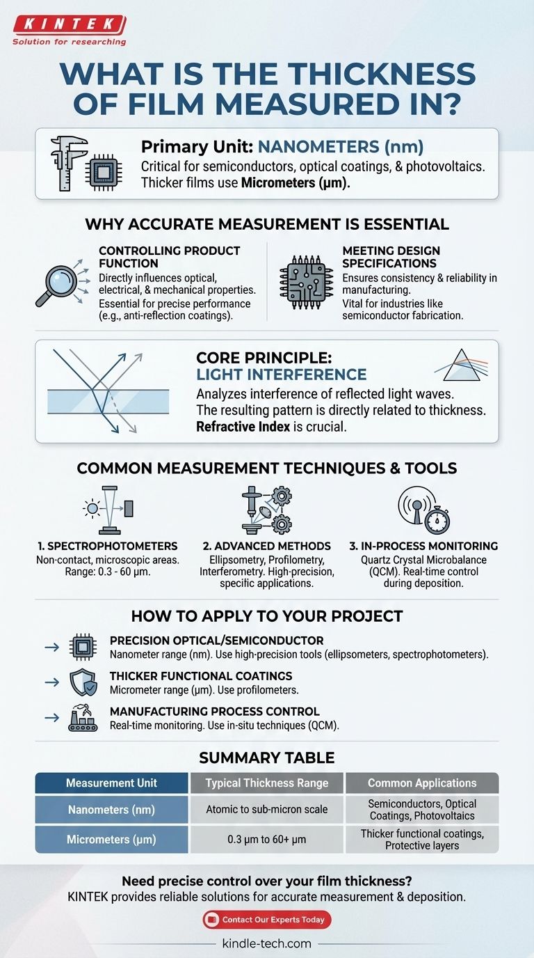
In most technical applications, the thickness of a thin film is measured in nanometers (nm). This unit is standard for materials used in semiconductors, optical coatings, and photovoltaics, where precision at the atomic level is critical for performance. For thicker films or coatings, measurements may also be expressed in microns (µm).
The core principle to understand is that the choice of measurement unit—and the technique used to obtain it—is dictated entirely by the film's intended function and its physical thickness. While nanometers are common for "thin" films, the broader context involves a range of tools and scales.
Why Accurate Thickness Measurement is Essential
Controlling Product Function
The thickness of a film is not an arbitrary dimension; it is a critical design parameter. It directly influences a product's optical, electrical, and mechanical properties.
For example, in anti-reflection coatings on lenses, the thickness must be precisely controlled to cancel out specific wavelengths of light. Any deviation compromises its function.
Meeting Design Specifications
Manufacturing processes require tight quality control to ensure consistency and reliability. Measuring film thickness verifies that the final product meets its design specifications and will perform as expected.
This is fundamental in industries like semiconductor fabrication, where even a slight variation in a dielectric layer can render a microchip useless.
The Core Principle of Measurement: Light Interference
How It Works
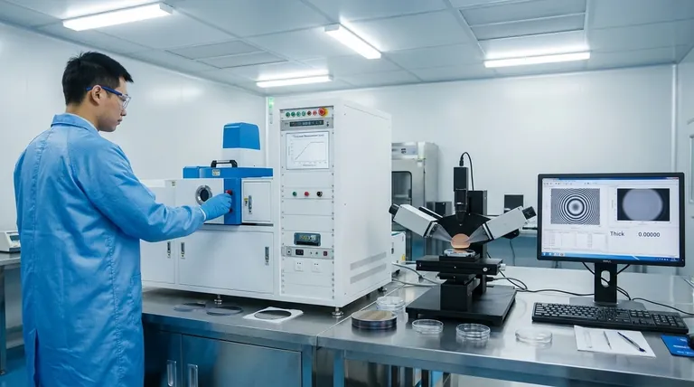
Many non-contact measurement tools operate by analyzing the interference of light. A beam of light is directed at the film, and reflections occur at both the top surface and the bottom interface.
These two reflected light waves interfere with each other. The resulting pattern of peaks and valleys in the light's spectrum is directly related to the thickness of the film.
The Role of Refractive Index
To calculate the final thickness from the interference pattern, you must know the material's refractive index. This property describes how light travels through that specific material.
Because every material has a different refractive index, it is a crucial variable in the calculation for ensuring an accurate measurement.
Common Measurement Techniques and Tools
Spectrophotometers
Spectrophotometers are a common non-contact tool for measuring film thickness. They are highly effective for microscopic sampling areas.
These instruments can typically measure layer thicknesses in the range of 0.3 to 60 micrometers (µm), making them versatile for both thin and relatively thick films.
Other Advanced Methods
Beyond spectrophotometry, several other high-precision techniques are used, including ellipsometry, profilometry, and interferometry. Each offers unique advantages depending on the material and application.
In-Process Monitoring
For real-time control during the manufacturing process, techniques like quartz crystal microbalance (QCM) sensors are used. These tools measure film thickness as it is being deposited, allowing for immediate adjustments.
How to Apply This to Your Project
A clear understanding of your goal is the most important factor in selecting the right measurement approach.
- If your primary focus is on precision optical coatings or semiconductor layers: You will be working in the nanometer (nm) range and require high-precision tools like ellipsometers or spectrophotometers.
- If your primary focus is on thicker functional coatings (e.g., protective layers): Measurements in micrometers (µm) are often sufficient, and tools like profilometers may be more practical.
- If your primary focus is on manufacturing process control: In-situ techniques like QCM are essential for real-time monitoring and adjustment during deposition.
Ultimately, mastering film thickness measurement is about translating a physical dimension into functional control.
Summary Table:
| Measurement Unit | Typical Thickness Range | Common Applications |
|---|---|---|
| Nanometers (nm) | Atomic to sub-micron scale | Semiconductors, Optical Coatings, Photovoltaics |
| Micrometers (µm) | 0.3 µm to 60+ µm | Thicker functional coatings, Protective layers |
Need precise control over your film thickness? KINTEK specializes in lab equipment and consumables, providing reliable solutions for accurate thickness measurement and deposition. Whether you're working with nanometer-scale semiconductors or thicker protective coatings, our expertise ensures your lab achieves consistent, high-quality results. Contact our experts today to discuss your specific application and find the perfect tool for your needs!
Visual Guide
Related Products
- Small Lab Rubber Calendering Machine
- Battery Lab Equipment 304 Stainless Steel Strip Foil 20um Thick for Battery Test
- Custom PTFE Teflon Parts Manufacturer for PTFE Measuring Cylinder 10/50/100ml
- Lab Plastic PVC Calender Stretch Film Casting Machine for Film Testing
People Also Ask
- What is the sputtering yield of materials? Master Deposition Rates & Film Quality
- What is the principle of wiped film molecular still? Preserve and Purify Heat-Sensitive Compounds
- What are the factors affecting sputtering yield? Master Your Deposition Rate & Film Quality
- What finishes are done using calendering technique? Achieve High Gloss, Embossing, and More
- What is a calendering machine? Transform Material Surfaces with Precision