Knowledge What is the thin film deposition method? A Guide to PVD & CVD Techniques
Author avatar

Tech Team · Kintek Solution

Updated 2 weeks ago

What is the thin film deposition method? A Guide to PVD & CVD Techniques

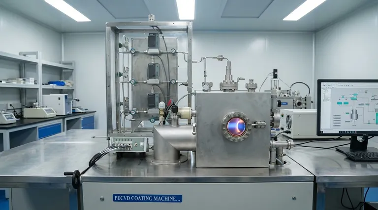
In essence, thin film deposition is a set of processes used to apply an extremely thin layer of material, often just a few atoms or molecules thick, onto a surface called a substrate. These methods are fundamental to manufacturing advanced products, from computer chips to solar panels, by giving the substrate new physical or chemical properties.

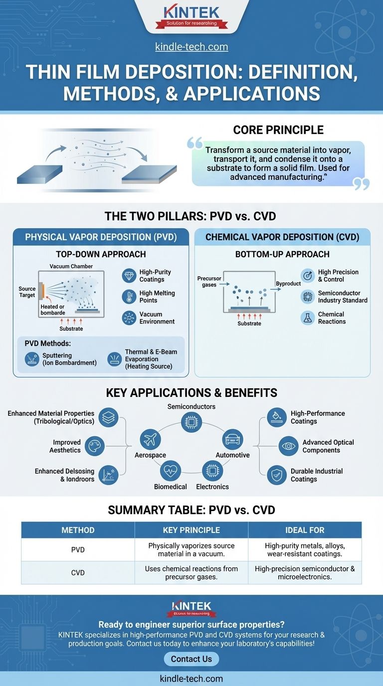
The core principle of thin film deposition is to transform a source material into a vapor, transport it, and then condense it onto a substrate to form a solid film. The two dominant methods to achieve this are Physical Vapor Deposition (PVD), which uses physical means like evaporation, and Chemical Vapor Deposition (CVD), which uses chemical reactions.

The Two Pillars of Deposition: PVD vs. CVD

At a high level, all thin film deposition techniques fall into one of two major categories: Physical Vapor Deposition (PVD) or Chemical Vapor Deposition (CVD). The choice between them is driven by the material being deposited and the desired properties of the final film.

Physical Vapor Deposition (PVD)

PVD is a "top-down" approach where a solid or liquid source material is physically transformed into a vapor, which then condenses onto the substrate. This process is always conducted in a vacuum to prevent the vapor from reacting with air.

PVD is typically used for materials with high melting points and when a high-purity coating is required.

Chemical Vapor Deposition (CVD)

CVD is a "bottom-up" approach where precursor gases are introduced into a chamber. These gases react or decompose on the surface of the substrate to create the desired solid film.

CVD is the most commonly used method in the semiconductor industry because it offers exceptionally high precision and control over the film's structure and thickness.

A Closer Look at PVD Methods

Because PVD encompasses several distinct techniques, it's helpful to understand the most common ones. The primary goal is always to generate atomic particles from a source target that can then coat the substrate.

Sputtering

Sputtering, sometimes called cathodic spraying, involves bombarding the source material (the "target") with high-energy ions. This collision physically knocks atoms loose from the target, which then travel and deposit onto the substrate.

Thermal & E-Beam Evaporation

Evaporation involves heating a source material until it reaches its boiling point and turns into a vapor. This vapor then travels through the vacuum chamber and condenses on the cooler substrate, forming the film. The heating can be done with a thermal source or a more focused electron beam (e-beam).

Understanding the Trade-offs

Choosing the right deposition method is a critical decision based on balancing cost, material properties, and the final application's requirements.

When to Choose CVD

CVD is the preferred method when precision is paramount. Its ability to grow a film atom-by-atom makes it ideal for the complex, layered structures found in microelectronics and semiconductors.

When to Choose PVD

PVD methods like sputtering are often chosen for depositing pure metals, alloys, and certain ceramic compounds. They are excellent for applications requiring hard, wear-resistant, or optically-specific coatings on tools, glass, and other components.

The Critical Role of the Source

Regardless of the method, the choice of the deposition source itself is key. Sources can include ion beams, magnetron sputtering cathodes, or thermal evaporators. The selection depends entirely on the materials you need to deposit and the final film characteristics you want to achieve.

Why This Process Matters: Key Applications

Thin film deposition is not an academic exercise; it is a foundational technology that enables a vast range of modern products and industries.

Enhancing Material Properties

A primary goal of deposition is to change the surface properties of an object. This includes improving tribological behavior (wear and friction resistance), enhancing optics (like anti-reflective coatings on lenses), or simply upgrading the aesthetics of a product.

Enabling Modern Technology

The impact of thin film deposition is widespread across numerous fields. It is essential for the semiconductor, aerospace, automotive, biomedical, and electronics industries, forming the basis for integrated circuits, durable engine components, and medical implants.

Making the Right Choice for Your Goal

To select the appropriate method, you must first define your primary objective.

  • If your primary focus is extreme precision and conformity for electronics: CVD is the established industry standard for its atomic-level control.
  • If your primary focus is creating a high-purity or high-melting-point coating: A PVD method like sputtering or e-beam evaporation is your most direct and effective path.
  • If your primary focus is a specific functional property like wear resistance: The choice will be driven by the specific material required for that property, which in turn will dictate whether a PVD or CVD process is more suitable.

Ultimately, mastering thin film deposition is about using atomic-scale engineering to build macro-scale performance.

Summary Table:

Method Key Principle Ideal For
PVD (Physical Vapor Deposition) Physically vaporizes a source material in a vacuum to coat a substrate. High-purity metals, alloys, and wear-resistant coatings.
CVD (Chemical Vapor Deposition) Uses chemical reactions from precursor gases to grow a film on a substrate. High-precision applications in semiconductors and microelectronics.

Ready to engineer superior surface properties with the right thin film deposition method?

At KINTEK, we specialize in providing high-performance lab equipment, including PVD and CVD systems, tailored to your specific research and production goals. Whether you are developing advanced semiconductors, durable industrial coatings, or cutting-edge optical components, our expertise ensures you achieve precise, reliable, and high-quality results.

Contact us today to discuss how our solutions can enhance your laboratory's capabilities and drive your innovations forward.

Related Products

People Also Ask

Related Products

Inclined Rotary Plasma Enhanced Chemical Vapor Deposition PECVD Equipment Tube Furnace Machine

Inclined Rotary Plasma Enhanced Chemical Vapor Deposition PECVD Equipment Tube Furnace Machine

Upgrade your coating process with PECVD coating equipment. Ideal for LED, power semiconductors, MEMS and more. Deposits high-quality solid films at low temps.

HFCVD Machine System Equipment for Drawing Die Nano-Diamond Coating

HFCVD Machine System Equipment for Drawing Die Nano-Diamond Coating

The nano-diamond composite coating drawing die uses cemented carbide (WC-Co) as the substrate, and uses the chemical vapor phase method ( CVD method for short ) to coat the conventional diamond and nano-diamond composite coating on the surface of the inner hole of the mold.

915MHz MPCVD Diamond Machine Microwave Plasma Chemical Vapor Deposition System Reactor

915MHz MPCVD Diamond Machine Microwave Plasma Chemical Vapor Deposition System Reactor

915MHz MPCVD Diamond Machine and its multi-crystal effective growth, the maximum area can reach 8 inches, the maximum effective growth area of single crystal can reach 5 inches. This equipment is mainly used for the production of large-size polycrystalline diamond films, the growth of long single crystal diamonds, the low-temperature growth of high-quality graphene, and other materials that require energy provided by microwave plasma for growth.

Vacuum Hot Press Furnace Machine for Lamination and Heating

Vacuum Hot Press Furnace Machine for Lamination and Heating

Experience clean and precise lamination with Vacuum Lamination Press. Perfect for wafer bonding, thin-film transformations, and LCP lamination. Order now!

Laboratory CVD Boron Doped Diamond Materials

Laboratory CVD Boron Doped Diamond Materials

CVD boron-doped diamond: A versatile material enabling tailored electrical conductivity, optical transparency, and exceptional thermal properties for applications in electronics, optics, sensing, and quantum technologies.

Laboratory Quartz Tube Furnace Tubular RTP Heating Furnace

Laboratory Quartz Tube Furnace Tubular RTP Heating Furnace

Get lightning-fast heating with our RTP Rapid Heating Tube Furnace. Designed for precise, high-speed heating and cooling with convenient sliding rail and TFT touch screen controller. Order now for ideal thermal processing!

Small Vacuum Heat Treat and Tungsten Wire Sintering Furnace

Small Vacuum Heat Treat and Tungsten Wire Sintering Furnace

The small vacuum tungsten wire sintering furnace is a compact experimental vacuum furnace specially designed for universities and scientific research institutes. The furnace features a CNC welded shell and vacuum piping to ensure leak-free operation. Quick-connect electrical connections facilitate relocation and debugging, and the standard electrical control cabinet is safe and convenient to operate.

Vacuum Heat Treat and Molybdenum Wire Sintering Furnace for Vacuum Sintering

Vacuum Heat Treat and Molybdenum Wire Sintering Furnace for Vacuum Sintering

A vacuum molybdenum wire sintering furnace is a vertical or bedroom structure, which is suitable for withdrawal, brazing, sintering and degassing of metal materials under high vacuum and high temperature conditions. It is also suitable for dehydroxylation treatment of quartz materials.

Graphite Vacuum Furnace High Thermal Conductivity Film Graphitization Furnace

Graphite Vacuum Furnace High Thermal Conductivity Film Graphitization Furnace

The high thermal conductivity film graphitization furnace has uniform temperature, low energy consumption and can operate continuously.

Vacuum Heat Treat Furnace with Ceramic Fiber Liner

Vacuum Heat Treat Furnace with Ceramic Fiber Liner

Vacuum furnace with polycrystalline ceramic fiber insulation liner for excellent heat insulation and uniform temperature field. Choose from 1200℃ or 1700℃ max. working temperature with high vacuum performance and precise temperature control.

High Temperature Muffle Oven Furnace for Laboratory Debinding and Pre Sintering

High Temperature Muffle Oven Furnace for Laboratory Debinding and Pre Sintering

KT-MD High temperature debinding and pre-sintering furnace for ceramic materials with various molding processes. Ideal for electronic components such as MLCC and NFC.

Graphite Vacuum Furnace IGBT Experimental Graphitization Furnace

Graphite Vacuum Furnace IGBT Experimental Graphitization Furnace

IGBT experimental graphitization furnace, a tailored solution for universities and research institutions, with high heating efficiency, user-friendliness, and precise temperature control.

Vacuum Dental Porcelain Sintering Furnace

Vacuum Dental Porcelain Sintering Furnace

Get precise and reliable results with KinTek's Vacuum Porcelain Furnace. Suitable for all porcelain powders, it features hyperbolic ceramic furnace function, voice prompt, and automatic temperature calibration.

Molybdenum Vacuum Heat Treat Furnace

Molybdenum Vacuum Heat Treat Furnace

Discover the benefits of a high-configuration molybdenum vacuum furnace with heat shield insulation. Ideal for high-purity, vacuum environments like sapphire crystal growth and heat treatment.

Vacuum Sealed Continuous Working Rotary Tube Furnace Rotating Tube Furnace

Vacuum Sealed Continuous Working Rotary Tube Furnace Rotating Tube Furnace

Experience efficient material processing with our vacuum-sealed rotary tube furnace. Perfect for experiments or industrial production, equipped with optional features for controlled feeding and optimized results. Order now.

1700℃ Muffle Oven Furnace for Laboratory

1700℃ Muffle Oven Furnace for Laboratory

Get superior heat control with our 1700℃ Muffle Furnace. Equipped with intelligent temperature microprocessor, TFT touch screen controller & advanced insulation materials for precise heating up to 1700C. Order now!

Laboratory Sterilizer Lab Autoclave Pulse Vacuum Lifting Sterilizer

Laboratory Sterilizer Lab Autoclave Pulse Vacuum Lifting Sterilizer

The pulse vacuum lifting sterilizer is a state-of-the-art equipment for efficient and precise sterilization. It uses pulsating vacuum technology, customizable cycles, and a user-friendly design for easy operation and safety.

Anti-Cracking Press Mold for Lab Use

Anti-Cracking Press Mold for Lab Use

The anti-cracking press mold is a specialized equipment designed for molding various shapes and sizes of film using high pressure and electric heating.

Laboratory Homogenizer Mixer Benchtop Homogenizer with 8 Inch PP Chamber

Laboratory Homogenizer Mixer Benchtop Homogenizer with 8 Inch PP Chamber

The 8-inch PP chamber laboratory homogenizer is a versatile and powerful piece of equipment designed for efficient homogenization and mixing of various samples in a laboratory setting. Constructed from durable materials, this homogenizer features a spacious 8-inch PP chamber, providing ample capacity for sample processing. Its advanced homogenization mechanism ensures thorough and consistent mixing, making it ideal for applications in fields such as biology, chemistry, and pharmaceuticals. With its user-friendly design and reliable performance, the 8-inch PP chamber laboratory homogenizer is an indispensable tool for laboratories seeking efficient and effective sample preparation.

Laboratory Sterilizer Lab Autoclave Vertical Pressure Steam Sterilizer for Liquid Crystal Display Automatic Type

Laboratory Sterilizer Lab Autoclave Vertical Pressure Steam Sterilizer for Liquid Crystal Display Automatic Type

Liquid crystal display automatic vertical sterilizer is a safe, reliable and automatic control sterilization equipment, which is composed of heating system, microcomputer control system and overheating and overvoltage protection system.


Leave Your Message