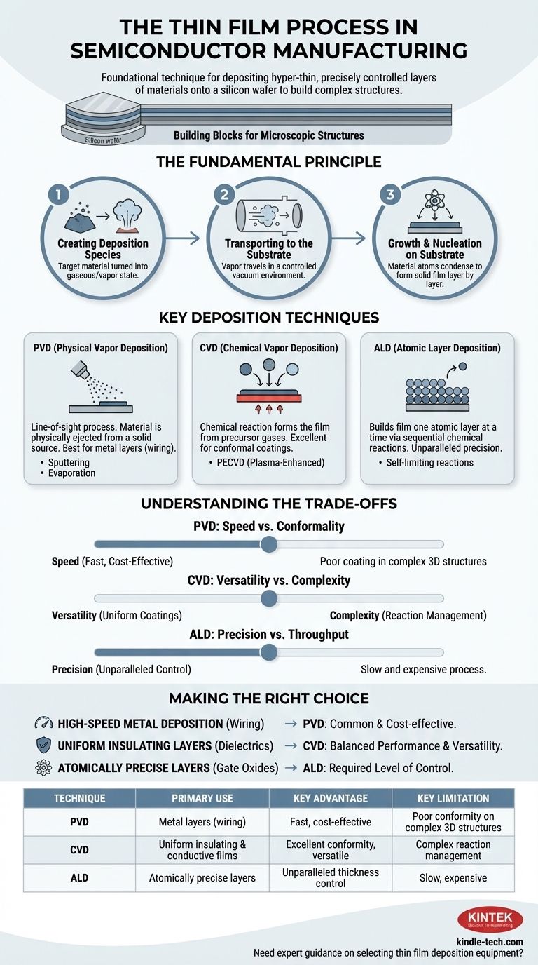
In short, the thin film process is the foundational technique in semiconductor manufacturing for depositing hyper-thin, precisely controlled layers of various materials onto a silicon wafer. This is not a single method, but a family of sophisticated techniques that systematically build up the complex, multi-layered structures that form transistors and integrated circuits. The entire process happens in a vacuum or controlled environment to ensure absolute purity and precision.
The core challenge in semiconductor fabrication is building microscopic, three-dimensional structures. Thin film deposition provides the essential "building blocks" by adding materials one layer at a time, with the choice of technique—primarily PVD, CVD, or ALD—dictated by the required precision, material, and cost for that specific layer.
The Fundamental Principle of Thin Film Growth
Before examining specific techniques, it's crucial to understand that all thin film deposition follows the same three-stage principle. This universal process is the foundation for creating every layer on a modern chip.
Step 1: Creating Deposition Species
The process begins by creating a source of the desired material in a gaseous or vapor state. This "target material" might be liberated from a solid source through evaporation or sputtering, or it may be introduced as a reactive precursor gas.
Step 2: Transporting to the Substrate
Once the material is in a vapor state, it must be transported to the surface of the silicon wafer (the substrate). This occurs within a highly controlled vacuum chamber to prevent contamination from unwanted particles or atmospheric gases.
Step 3: Growth and Nucleation on the Substrate
When the material atoms or molecules arrive at the wafer's surface, they condense and begin to form a solid film. This growth process, known as nucleation, builds up the material layer by layer until the desired thickness is achieved.
Key Deposition Techniques Explained
While the core principle is the same, the method used to create and transport the material defines the specific technique. The three most critical methods in semiconductor manufacturing are Physical Vapor Deposition (PVD), Chemical Vapor Deposition (CVD), and Atomic Layer Deposition (ALD).
Physical Vapor Deposition (PVD)
PVD is a "line-of-sight" process. Think of it as an atomic-scale spray-painting technique.
Material is physically ejected from a solid source (the target) and travels in a straight line to coat the wafer. This is typically done through sputtering (bombarding the target with ions) or evaporation (heating the target until it vaporizes).
Chemical Vapor Deposition (CVD)
CVD relies on a chemical reaction to form the film. One or more reactive precursor gases are introduced into a chamber containing the wafer.
When these gases reach the heated wafer surface, they react and decompose, leaving behind a solid film of the desired material. A common variant is Plasma-Enhanced CVD (PECVD), which uses plasma to drive the reaction at lower temperatures.
Atomic Layer Deposition (ALD)
ALD is the most precise method available, building the film literally one single atomic layer at a time.
The process uses a sequence of self-limiting chemical reactions. A precursor gas is pulsed into the chamber, coating the entire surface with exactly one layer of molecules. Any excess is purged, and a second gas is introduced to react with the first layer, completing the atomic film. This cycle is repeated hundreds or thousands of times.
Understanding the Trade-offs
No single deposition method is perfect for every application. Engineers choose the right tool for the job based on a clear set of trade-offs between speed, precision, and cost.
PVD: Speed vs. Conformality
PVD is often fast and relatively inexpensive, making it ideal for depositing metal layers for wiring (interconnects). However, because it's a line-of-sight process, it struggles to evenly coat the inside of deep, narrow trenches and other complex 3D structures.
CVD: Versatility vs. Complexity
CVD is highly versatile and excellent at creating uniform, "conformal" coatings over complex topographies. It's used for many different dielectric (insulating) and conductive films. The primary trade-off is the complexity of managing the chemical reactions to avoid impurities in the final film.
ALD: Precision vs. Throughput
ALD offers unparalleled control over film thickness and uniformity, making it essential for creating the ultra-thin gate oxides and other critical layers in advanced transistors. Its major drawback is that it is an extremely slow and expensive process, reserved only for layers where absolute precision is non-negotiable.
Making the Right Choice for Your Application
The selection of a thin film process is a critical engineering decision driven entirely by the goal for a specific layer within the semiconductor device.
- If your primary focus is high-speed metal deposition for wiring: PVD is the most common and cost-effective choice.
- If your primary focus is creating high-quality, uniform insulating layers: CVD and its variants like PECVD offer the best balance of performance and versatility.
- If your primary focus is building atomically precise layers for cutting-edge transistors: ALD is the only technique that provides the required level of control.
Ultimately, mastering the interplay of these deposition techniques is what enables the relentless progress of modern electronics.
Summary Table:
| Technique | Primary Use | Key Advantage | Key Limitation |
|---|---|---|---|
| PVD (Physical Vapor Deposition) | Metal layers for wiring (interconnects) | Fast, cost-effective | Poor conformity on complex 3D structures |
| CVD (Chemical Vapor Deposition) | Uniform insulating & conductive films | Excellent conformity, versatile | Complex reaction management |
| ALD (Atomic Layer Deposition) | Atomically precise layers (e.g., gate oxides) | Unparalleled thickness control & uniformity | Slow, expensive |
Need expert guidance on selecting the right thin film deposition equipment for your semiconductor lab? KINTEK specializes in high-precision lab equipment and consumables, providing solutions tailored to your specific PVD, CVD, or ALD requirements. Our expertise ensures you achieve optimal layer uniformity, purity, and performance for cutting-edge semiconductor fabrication. Contact our specialists today to discuss how we can support your laboratory's advanced manufacturing needs!
Visual Guide
Related Products
- Versatile PTFE Solutions for Semiconductor and Medical Wafer Processing
- Vacuum Hot Press Furnace Machine for Lamination and Heating
- Custom PTFE Wafer Holders for Lab and Semiconductor Processing
- Customizable PTFE Wafer Carriers for Semiconductor and Lab Applications
- Thin-Layer Spectral Electrolysis Electrochemical Cell
People Also Ask
- What inspection should be performed on a PTFE cleaning basket before use? A 3-Step Protocol for Safe, Effective Cleaning
- What is the procedure for using a PTFE cleaning basket? A 3-Step Guide for Flawless Results
- What is the maximum operating temperature for a PTFE cleaning basket? Avoid Catastrophic Failure at 260°C
- What material is a PTFE cleaning basket made of? Unlocking Superior Chemical and Thermal Resistance
- What precautions should be taken regarding the physical handling and loading of a PTFE cleaning basket? Prevent Damage and Ensure Process Integrity