At its core, Chemical Vapor Deposition (CVD) is used to create highly durable and exceptionally uniform thin-film coatings on a surface. This is not a simple layer of paint; it is a chemical process that builds a new, functional layer directly onto a substrate, molecule by molecule. This allows it to enhance a material's properties—like wear resistance—or to build the fundamental components of electronic devices.
The essential purpose of CVD is to fundamentally alter a component's surface by chemically bonding a new, high-performance layer to it. This makes it a foundational process for industries that demand extreme durability and functional precision, such as in high-wear tooling and semiconductor manufacturing.
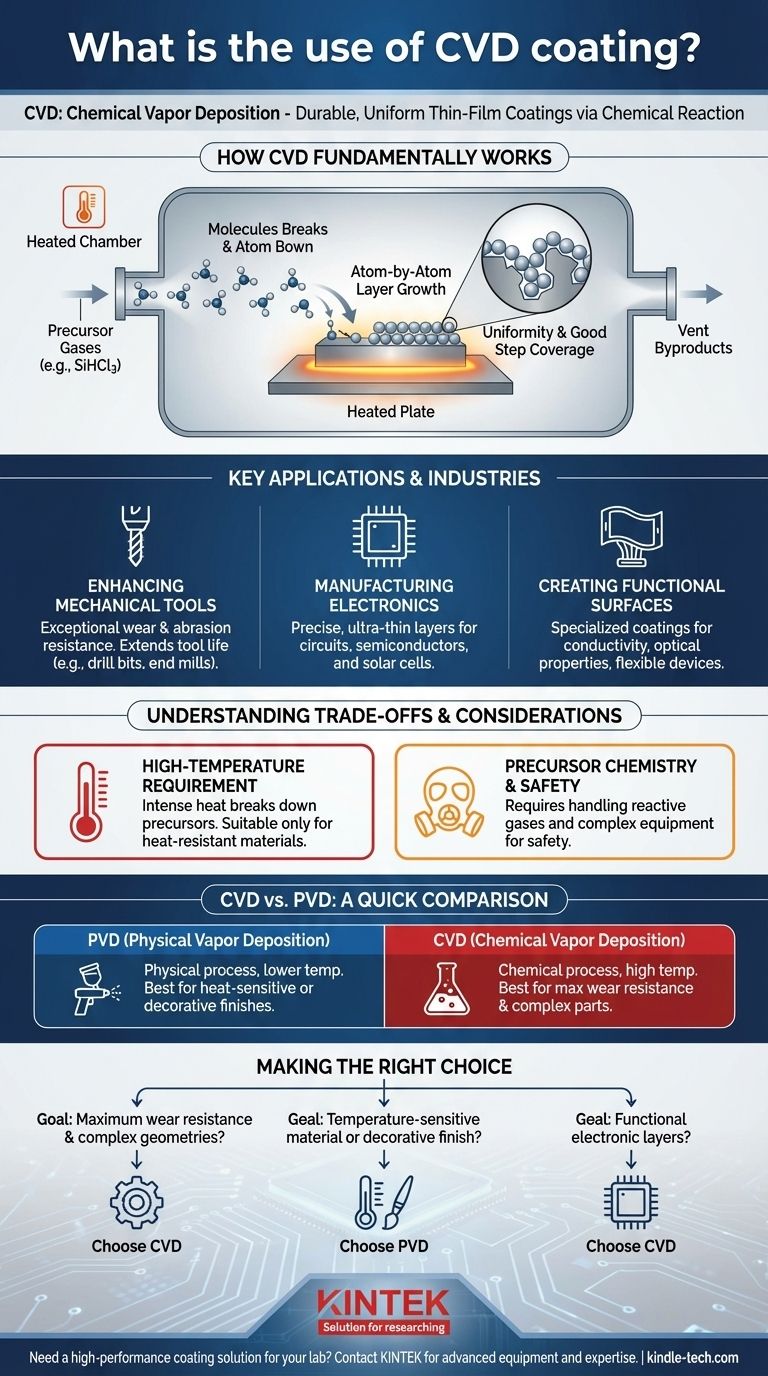
How CVD Fundamentally Works
The Concept of Chemical Reaction
Unlike physical coatings that are simply applied to a surface, CVD involves a chemical reaction. The process takes place inside a heated chamber where specific gases, known as precursors, are introduced.
Building a Layer Atom by Atom
These precursor gases react or decompose on the hot surface of the object being coated. For example, to create a silicon coating, trichlorosilane (SiHCl3) gas can be used. When heated, it breaks down, and the silicon atoms bond directly to the substrate, forming a new, dense, and uniform layer.
Uniformity is Key
Because the precursor is a gas, it can flow into and around complex shapes, coating all surfaces evenly. This ability to uniformly coat intricate geometries, a characteristic known as good step coverage, is one of CVD's primary advantages. Unwanted chemical byproducts, like hydrochloric acid gas in the silicon example, are safely vented away.
Key Applications and Industries
The unique properties of CVD coatings make them critical for several high-performance applications.
Enhancing Mechanical Tools
CVD coatings are exceptionally resistant to abrasion and wear, often more so than Physical Vapor Deposition (PVD) coatings. This makes them ideal for extending the life of cutting tools and components that face extreme friction, such as drill bits and end mills.
Manufacturing Electronics and Semiconductors
CVD is a cornerstone of the electronics industry. It is used to deposit the ultra-thin, precise layers required for modern devices. These include dielectric films like silicon dioxide (SiO2) and silicon nitride (Si3N4) that insulate circuits, as well as the semiconductor films that form the active parts of microchips and solar cells.
Creating Protective and Functional Surfaces
The process is also used to apply specialized coatings for other purposes. For instance, tin oxide coatings can be deposited to create layers with specific conductive or optical properties, essential in devices like flexible displays and sensors.
Understanding the Trade-offs and Considerations
While powerful, CVD is not a universal solution. Its process characteristics create specific limitations that must be understood.
The High-Temperature Requirement
The chemical reactions in CVD require very high temperatures. This heat is necessary to break down the precursor gases and create a strong chemical bond with the substrate. A significant consequence is that CVD is only suitable for materials that can withstand this intense heat without deforming or losing their structural integrity.
Precursor Chemistry and Safety
CVD relies on volatile and often reactive precursor gases. Managing these chemicals, along with their byproducts, requires sophisticated equipment for safe handling, venting, and scrubbing to comply with regulatory standards. This adds complexity to the manufacturing process.
CVD vs. PVD: A Quick Comparison
The references frequently mention PVD, making it a useful comparison. PVD is a physical process (like atomic-scale spray painting) that typically runs at lower temperatures. Because of this, PVD is often used for heat-sensitive materials or for decorative finishes on consumer goods like faucets, jewelry, and automotive components. CVD, in contrast, is chosen when the absolute highest wear resistance or perfect conformity on a complex part is the primary goal.
Making the Right Choice for Your Goal
Selecting the right coating technology depends entirely on the demands of your application and the material of your component.
- If your primary focus is maximum wear resistance and coating complex internal geometries: CVD is the superior choice due to its chemical bonding process and its ability to deposit a uniform layer on any exposed surface.
- If your primary focus is coating temperature-sensitive materials or achieving a specific decorative finish: PVD is often the better alternative because of its lower processing temperatures and wider range of aesthetic options.
- If your primary focus is building functional electronic layers for microchips or sensors: CVD is the industry-standard technology for depositing the precise, high-purity films required for these devices.
Ultimately, understanding the underlying chemical principles of CVD is the key to leveraging its unique advantages for your specific application.
Summary Table:
| Key Aspect | Description |
|---|---|
| Primary Use | Creating highly durable, uniform thin-film coatings via a chemical reaction. |
| Key Advantage | Exceptional wear resistance and uniform coverage on complex geometries. |
| Common Applications | Cutting tools, semiconductor devices, microchips, solar cells, sensors. |
| Main Consideration | Requires high processing temperatures, limiting use to heat-resistant materials. |
Need a high-performance coating solution for your lab equipment or components?
KINTEK specializes in providing advanced lab equipment and consumables. Whether you're developing cutting-edge electronics or require durable coatings for mechanical tools, our expertise can help you select the right technology for your specific application.
Contact our experts today to discuss how we can support your laboratory's coating and material science needs!
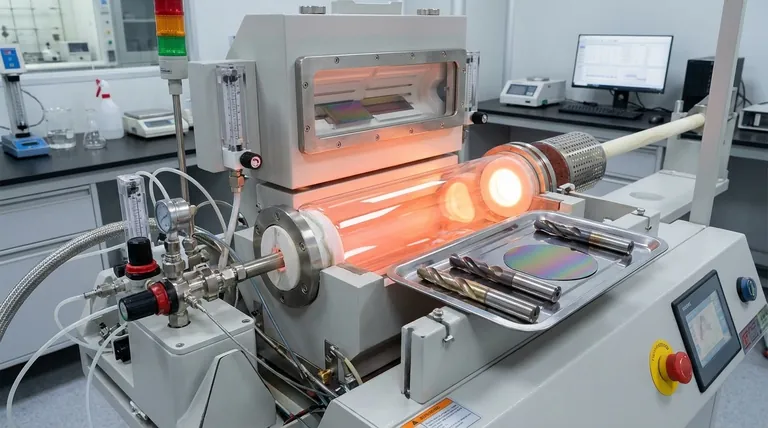
Visual Guide
Related Products
- Custom CVD Diamond Coating for Lab Applications
- HFCVD Machine System Equipment for Drawing Die Nano-Diamond Coating
- Laboratory CVD Boron Doped Diamond Materials
- CVD Diamond for Thermal Management Applications
- CVD Diamond Dressing Tools for Precision Applications
People Also Ask
- What are the different CVD coating? A Guide to Thermal CVD, PECVD, and Specialized Methods
- Can you coat something in diamond? Unlock Unmatched Hardness and Thermal Conductivity
- What are the types of CVD coating? A Guide to Choosing the Right Process
- How thick is CVD diamond coating? Balancing Durability and Stress for Optimal Performance
- What are the advantages of CVD coating? Superior Hardness and Uniformity for Demanding Applications


