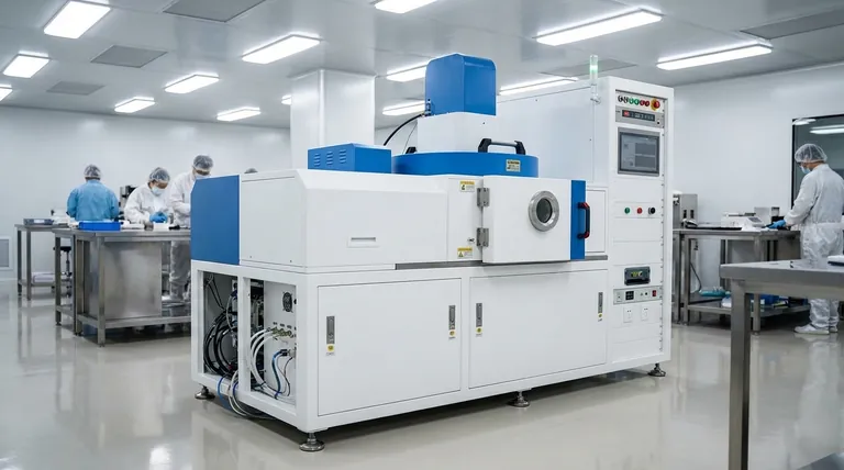
At its core, Physical Vapor Deposition (PVD) is a sophisticated vacuum coating process used to apply extremely thin, high-performance films of material onto a surface. These films are used to dramatically enhance the properties of a product, providing benefits like extreme hardness, corrosion resistance, thermal protection, or specific optical and electronic characteristics. Its applications span from aerospace and medical devices to cutting tools and semiconductors.
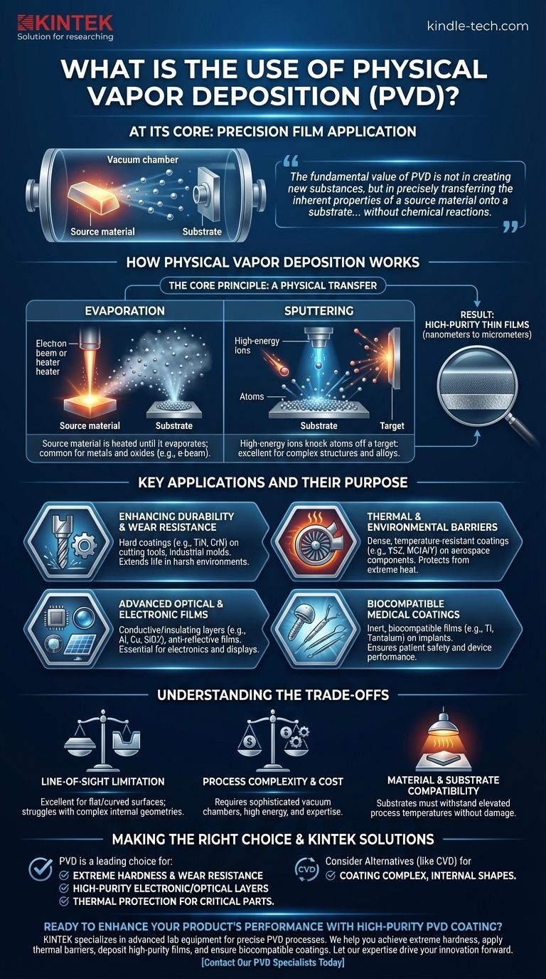
The fundamental value of PVD is not in creating new substances, but in precisely transferring the inherent properties of a source material onto a substrate. It physically moves atoms from a source to a target in a vacuum, creating a pure, dense, and functional surface layer without chemical reactions.
How Physical Vapor Deposition Works
To understand the use of PVD, you must first understand its fundamental mechanism. The process is defined by what it doesn't do: it does not rely on chemical reactions.
The Core Principle: A Physical Transfer
All PVD processes occur inside a high-vacuum chamber. First, a source material—often a metal, alloy, or ceramic—is converted into a vapor. This vapor then travels through the vacuum and condenses onto the target object (the substrate), forming a solid, tightly bonded film.
Because this happens in a vacuum, the process is extremely clean, preventing contaminants from being trapped in the coating.
Evaporation vs. Sputtering
There are two primary methods for creating the vapor:
- Evaporation: The source material is heated until it essentially boils and evaporates. Electron-beam (e-beam) evaporation is a common technique used to deposit a wide range of materials, including metals and even oxides.
- Sputtering: The source material (the "target") is bombarded with high-energy ions. This impact physically knocks atoms off the target's surface, ejecting them toward the substrate in a process akin to an atomic-scale sandblaster.
The Result: High-Purity Thin Films
The result is a deposited film that can be anywhere from a few nanometers to several micrometers thick. Because it is a physical transfer of the source material, the resulting film is exceptionally pure and dense, accurately reflecting the properties of the material it came from.
This process can also be controlled to create complex structures, including multiple layers of different materials or films with a graded composition.
Key Applications and Their Purpose
The versatility of PVD allows it to solve critical challenges across numerous high-tech industries. The application is determined by the properties of the material being deposited.
Enhancing Durability and Wear Resistance
Hard materials like titanium nitride can be sputtered onto cutting tools, drills, and industrial molds. This creates a hard, corrosion-resistant coating that dramatically extends the life and performance of tools used in harsh environments.
Thermal and Environmental Barriers
In the aerospace industry, PVD is used to apply dense, temperature-resistant coatings to components like turbine blades. These thermal barrier coatings protect the underlying parts from the extreme temperatures of a jet engine, improving durability and safety.
Advanced Optical and Electronic Films
The precision of PVD makes it essential for electronics. It is used to deposit the conductive metal layers on semiconductors, create anti-reflective optical films for solar panels and lenses, and even produce the reflective layers used in holographic displays.
Biocompatible Medical Coatings
PVD is used to apply inert and biocompatible coatings to medical implants, surgical tools, and other devices. These films ensure the device does not react with the body, improving patient safety and device performance.
Understanding the Trade-offs
While powerful, PVD is not a universal solution. Understanding its limitations is key to using it effectively.
The "Line-of-Sight" Limitation
Because the vaporized atoms travel in a relatively straight line from the source to the substrate, PVD is a "line-of-sight" process. It is excellent for coating flat or externally curved surfaces but struggles to evenly coat complex, internal geometries or the inside of narrow tubes.
Process Complexity and Cost
PVD requires sophisticated and expensive equipment, including high-vacuum chambers and high-energy power sources. The process requires significant expertise to control variables like temperature, pressure, and deposition rate to achieve the desired film properties.
Material and Substrate Compatibility
While versatile, not all materials can be easily deposited with PVD. Furthermore, the process often involves elevated temperatures, which means the substrate material must be able to withstand the heat without deforming or being damaged.
Making the Right Choice for Your Goal
Selecting a coating technology depends entirely on your desired outcome. Use these points as a guide.
- If your primary focus is extreme hardness and wear resistance: PVD is a leading choice for applying hard, ceramic-like coatings onto tools and components.
- If your primary focus is high-purity electronic or optical layers: The precision and low-contamination environment of PVD make it superior for semiconductors, sensors, and optical applications.
- If your primary focus is thermal protection for critical parts: PVD is the industry standard for creating the dense thermal barrier coatings essential for aerospace and high-performance engines.
- If your primary focus is coating complex, internal shapes: You may need to investigate alternatives like Chemical Vapor Deposition (CVD), which can more easily coat non-line-of-sight surfaces.
Ultimately, PVD is about leveraging a material's inherent strengths by precisely transferring them onto the surface of another.
Summary Table:
| Key Application | Primary Purpose | Common Materials Deposited |
|---|---|---|
| Cutting Tools & Industrial Parts | Extreme Hardness & Wear Resistance | Titanium Nitride (TiN), Chromium Nitride (CrN) |
| Aerospace Components | Thermal Barrier & Corrosion Protection | Yttria-Stabilized Zirconia (YSZ), MCrAlY Alloys |
| Semiconductors & Electronics | Conductive & Insulating Layers | Aluminum, Copper, Silicon Dioxide |
| Medical Implants & Devices | Biocompatibility & Corrosion Resistance | Titanium, Tantalum, Nitinol |
| Optical Lenses & Displays | Anti-Reflective & Reflective Coatings | Magnesium Fluoride, Silver, Silicon Nitride |
Ready to enhance your product's performance with a high-purity PVD coating?
At KINTEK, we specialize in providing advanced lab equipment and consumables for precise Physical Vapor Deposition processes. Whether you are developing cutting-edge semiconductors, durable medical devices, or high-performance aerospace components, our solutions ensure superior film quality, adhesion, and consistency.
We help you:
- Achieve extreme surface hardness to extend the life of your tools and components.
- Apply thermal barrier coatings to protect critical parts in high-temperature environments.
- Deposit high-purity conductive or optical films for advanced electronic and display applications.
- Ensure biocompatible coatings for medical implants and surgical instruments.
Let our expertise in vacuum coating technology drive your innovation forward. Contact our PVD specialists today to discuss your specific application requirements and discover the right solution for your laboratory needs.
Visual Guide
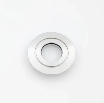
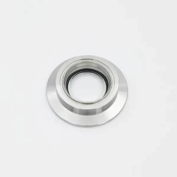
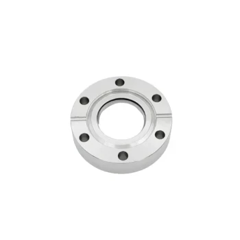
Related Products
- Variable Speed Peristaltic Pump
- Optical Water Bath Electrolytic Electrochemical Cell
- Chemical Vapor Deposition CVD Equipment System Chamber Slide PECVD Tube Furnace with Liquid Gasifier PECVD Machine
- Vacuum Cold Mounting Machine for Sample Preparation
- Round Bidirectional Press Mold for Lab
People Also Ask
- What function does a 0.45 μm syringe filter perform for Chlorendic Acid samples? Secure Accurate Reaction Kinetics
- What chemicals are used in heat treatment? Master the Quenching Process for Optimal Metal Properties
- What is the role of a gas purification unit in the SHS process? Ensure Pristine Metal Dispersion & Film Stability
- What is sputtering rate? Master the Key to Controlling Thin Film Deposition Speed
- Why is a capacitance manometer preferred for RF plasma systems? Ensure Precise Gas-Independent Pressure Monitoring