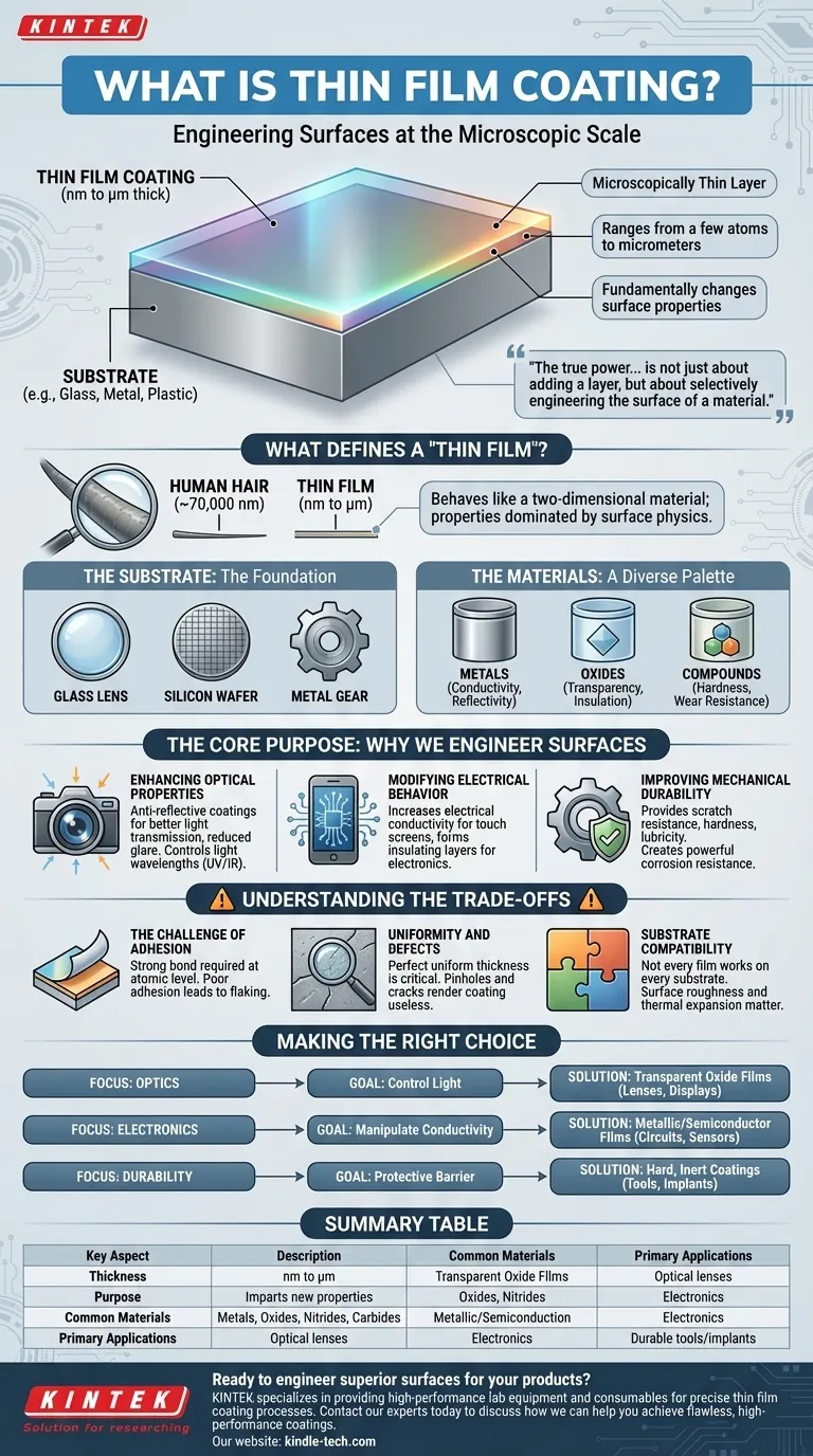
In essence, a thin film coating is an microscopically thin layer of material, ranging from a few atoms to several micrometers thick, that is applied to the surface of an object called a substrate. This process is not like painting; it's a highly controlled engineering method used to fundamentally change the surface properties of the base material—such as glass, metal, or plastic—without altering its underlying structure. The film imparts new characteristics like scratch resistance, electrical conductivity, or anti-reflection.
The true power of thin film coating is not just about adding a layer, but about selectively engineering the surface of a material. It allows you to impart new, high-performance properties onto a base material without changing its core structure, creating a composite with the best attributes of both.

What Defines a "Thin Film"?
To understand thin film technology, you must first grasp its defining characteristics: its incredible thinness and its relationship with the base material.
The Scale: From Nanometers to Micrometers
A film is considered "thin" when its thickness is vastly smaller than its length and width, often measured in nanometers (nm) or micrometers (µm). For context, a human hair is about 70,000 nanometers thick.
Because the thickness is suppressed to this near-atomic scale, a thin film behaves almost like a two-dimensional material. Its properties are dominated by surface physics rather than the bulk characteristics of the material it's made from.
The Substrate: The Foundation
A thin film cannot exist on its own; it must be deposited onto a substrate. The substrate provides the mechanical structure and is the object whose properties are being enhanced.
Common substrates include glass for optical lenses, silicon wafers for microchips, and metals for cutting tools or medical implants.
The Materials: A Diverse Palette
The materials used to create the film are chosen specifically for the property you wish to impart. The palette is incredibly diverse and includes:
- Metals: Used for conductivity in electronics or reflectivity in mirrors.
- Oxides: Often used for their transparency, durability, and insulating properties, like the coatings on eyeglass lenses.
- Compounds: A broad category including nitrides and carbides, known for extreme hardness and wear resistance.
The Core Purpose: Why We Engineer Surfaces
Applying a thin film is a solution-oriented process. The goal is to solve a specific problem by modifying a material's surface to perform a function it couldn't perform on its own.
Enhancing Optical Properties
One of the most common applications is controlling light. By applying films of a precise thickness and refractive index, we can create anti-reflective coatings on camera lenses and eyeglasses, which improve light transmission and reduce glare.
Other optical films can be designed to block specific wavelengths of light, like UV or infrared, which is critical for sunglasses and architectural glass.
Modifying Electrical Behavior
Thin films are the bedrock of the modern electronics industry. They can be used to create pathways that increase electrical conductivity or form layers that act as electrical insulation.
Your smartphone's touch screen, for example, relies on a transparent, conductive thin film (often Indium Tin Oxide) to register your touch.
Improving Mechanical Durability
For mechanical parts, tools, and medical implants, durability is paramount. Thin film coatings can provide exceptional scratch resistance, hardness, and lubricity.
Furthermore, chemically inert films create a barrier that offers powerful corrosion resistance, dramatically extending the life of the underlying material.
Understanding the Trade-offs
While powerful, thin film coating is a precise science with inherent challenges. Success is not guaranteed and depends on overcoming several key hurdles.
The Challenge of Adhesion
A coating is only effective if it stays on the substrate. Achieving a strong, permanent bond between two dissimilar materials at the atomic level is a significant manufacturing challenge. Poor adhesion leads to flaking, peeling, and failure.
Uniformity and Defects
At the nanoscale, even minute imperfections matter. Ensuring the film has a perfectly uniform thickness across the entire surface is critical, especially for optical and electronic applications. Pinholes, cracks, or contaminants can render the coating useless.
Substrate Compatibility
Not every film material can be successfully deposited onto every substrate. Factors like surface roughness, cleanliness, and differences in thermal expansion can create stress and cause the film to fail. The choice of film and substrate must be a compatible pairing.
Making the Right Choice for Your Goal
Understanding the purpose of the coating is key to appreciating its application. The material and process are always dictated by the desired outcome.
- If your primary focus is optics (lenses, displays): Your goal is to control light, requiring transparent oxide films with specific refractive indices for anti-reflection or filtering.
- If your primary focus is electronics (circuits, sensors): You will be manipulating conductivity, using metallic or semiconductor films to create conductive pathways or insulating layers.
- If your primary focus is durability (tools, implants): You need hard, inert coatings like nitrides or carbides to provide a protective barrier against wear, corrosion, and friction.
Ultimately, thin film coating is the science of transforming an ordinary surface into an extraordinary one.
Summary Table:
| Key Aspect | Description |
|---|---|
| Thickness | Nanometers (nm) to micrometers (µm) |
| Purpose | Imparts new properties (e.g., scratch resistance, conductivity) to a substrate |
| Common Materials | Metals, Oxides, Nitrides, Carbides |
| Primary Applications | Optical lenses, Electronics, Durable tools/implants |
Ready to engineer superior surfaces for your products?
KINTEK specializes in providing the high-performance lab equipment and consumables essential for precise thin film coating processes. Whether you are developing advanced optics, durable components, or next-generation electronics, our solutions support the critical deposition and analysis steps needed for success.
Contact our experts today to discuss how we can help you achieve flawless, high-performance coatings.
Visual Guide
Related Products
- Aluminized Ceramic Evaporation Boat for Thin Film Deposition
- Electron Beam Evaporation Coating Oxygen-Free Copper Crucible and Evaporation Boat
- Tungsten Evaporation Boat for Thin Film Deposition
- Molybdenum Tungsten Tantalum Evaporation Boat for High Temperature Applications
- Aluminum-Plastic Flexible Packaging Film for Lithium Battery Packaging
People Also Ask
- Why is an alumina boat selected for catalyst precursors? Ensure Sample Purity at 1000 °C
- What is the chemical method for thin film deposition? Build Films from the Molecular Level Up
- What is the source of evaporation for thin film? Choosing Between Thermal and E-Beam Methods
- What are thin films deposited by evaporation? A Guide to High-Purity Coating
- What are the applications of thin films deposition? Unlock New Possibilities for Your Materials


