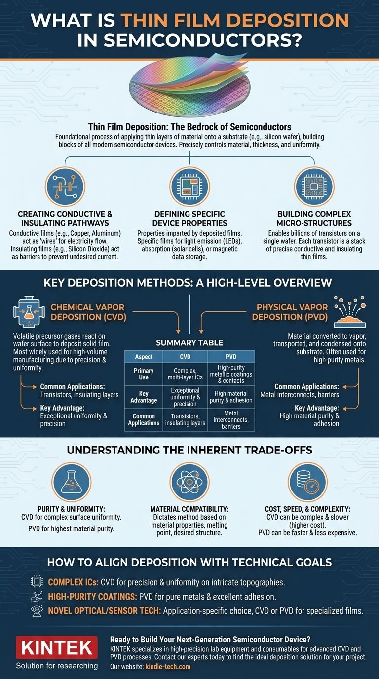
At its core, thin film deposition is the foundational process of applying incredibly thin layers of material onto a substrate, such as a silicon wafer. These layers, which can range from a few atoms to several micrometers in thickness, are the fundamental building blocks of all modern semiconductor devices. By precisely controlling the material, thickness, and uniformity of these films, engineers construct the intricate pathways and components that form integrated circuits, microprocessors, and memory chips.
Thin film deposition is not merely a coating technique; it is the essential architectural method for building electronic devices. It allows for the creation of complex, multi-layered structures that either conduct, insulate, or modify electrical current, which is the principle that underpins all of modern microelectronics.
Why Thin Films are the Bedrock of Semiconductors
To understand the importance of thin film deposition, one must think of it as constructing a multi-story building at a microscopic level. Each film is a new floor with a specific purpose, and their precise arrangement creates a functional, complex system.
Creating Conductive and Insulating Pathways
The primary function of a semiconductor device is to control the flow of electricity. Thin film deposition is how this control is achieved.
By depositing thin films of metals like copper or aluminum, engineers create conductive pathways, or "wires," that allow electricity to travel between components on the chip. Conversely, depositing films of insulators like silicon dioxide creates barriers that prevent electrical current from flowing where it shouldn't.
Defining Specific Device Properties
The properties of a semiconductor are not inherent to the silicon wafer alone; they are imparted by the deposited films.
The choice of material and the thickness of the deposited layer directly determine its function. A specific film might serve as a light-emitting layer in an LED, a light-absorbing layer in a solar cell, or a magnetic layer in a data storage device.
Building Complex Micro-Structures
A modern microprocessor contains billions of transistors. Each transistor is a tiny switch built from a specific stack of conductive and insulating thin films.
The ability to deposit these layers with extreme precision and repeat the process hundreds of times on a single wafer is what enables the creation of such dense and powerful integrated circuits.
Key Deposition Methods: A High-Level Overview
While there are numerous techniques, they generally fall into two major categories. The choice of method depends on the material being deposited, the required purity, and the desired structural properties of the film.
Chemical Vapor Deposition (CVD)
CVD is the most widely used method in high-volume semiconductor manufacturing due to its exceptional precision and ability to create highly uniform films.
In this process, the silicon wafer is exposed to one or more volatile precursor gases. A chemical reaction occurs on the wafer's surface, causing a solid material—the thin film—to be deposited.
Physical Vapor Deposition (PVD)
PVD describes a set of processes where a material is converted into a vapor, transported, and then condensed onto the substrate to form the thin film.
Common PVD techniques include sputtering, where a target material is bombarded with ions, ejecting atoms that then coat the wafer, and evaporation, where a material is heated in a vacuum until it vaporizes and condenses on the substrate. PVD is often used for depositing high-purity metals.
Understanding the Inherent Trade-offs
Selecting a deposition method is a critical engineering decision driven by a series of trade-offs. The "best" method is entirely dependent on the specific goal for that particular layer within the semiconductor device.
Purity and Uniformity
The ultimate goal is a perfectly uniform film, free of any defects or impurities, as even a single microscopic flaw can disable a transistor and render the entire chip useless. CVD is renowned for its uniformity over complex surfaces, while PVD is often chosen when the absolute highest material purity is the primary concern.
Material Compatibility
Not all materials can be deposited with every method. The chemical properties, melting point, and desired final structure of the material dictate which deposition techniques are viable. Some complex alloys can only be created with PVD, while certain compounds require the chemical reactions of CVD.
Cost, Speed, and Complexity
CVD processes can be more complex and slower, making them more expensive, but the precision they offer is non-negotiable for critical layers. PVD can sometimes be faster and less expensive, making it suitable for less critical layers like the metal contacts that connect the chip to the outside world.
How to Align Deposition with Technical Goals
Your understanding of thin film deposition should be framed by the intended outcome. Different applications demand different priorities, which in turn dictate the appropriate manufacturing approach.
- If your primary focus is creating complex, multi-layered integrated circuits: CVD is the dominant choice due to its unparalleled ability to deposit highly precise and uniform films over intricate topographies.
- If your primary focus is applying a high-purity metallic coating for contacts or barriers: PVD methods like sputtering are often ideal for their ability to deposit pure metals with excellent adhesion.
- If your primary focus is developing novel optical or sensor technologies: The choice is application-specific, as both CVD and PVD are used to create the specialized films required for lenses, solar cells, and advanced sensors.
Ultimately, mastering thin film deposition is the critical skill that transforms raw materials like silicon into the intelligent heart of modern technology.
Summary Table:
| Aspect | Chemical Vapor Deposition (CVD) | Physical Vapor Deposition (PVD) |
|---|---|---|
| Primary Use | Complex, multi-layer ICs | High-purity metallic coatings & contacts |
| Key Advantage | Exceptional uniformity & precision | High material purity & adhesion |
| Common Applications | Transistors, insulating layers | Metal interconnects, barriers |
Ready to Build Your Next-Generation Semiconductor Device?
The right thin film deposition process is critical to your chip's performance and yield. KINTEK specializes in providing the high-precision lab equipment and consumables needed for advanced CVD and PVD processes. Our expertise helps R&D teams and manufacturers achieve the material purity, uniformity, and complex layering required for cutting-edge semiconductors, MEMS, and optoelectronic devices.
Let's discuss your specific technical requirements. Contact our experts today to find the ideal deposition solution for your project.
Visual Guide
Related Products
- Aluminized Ceramic Evaporation Boat for Thin Film Deposition
- Tungsten Evaporation Boat for Thin Film Deposition
- Electron Beam Evaporation Coating Oxygen-Free Copper Crucible and Evaporation Boat
- Molybdenum Tungsten Tantalum Evaporation Boat for High Temperature Applications
- HFCVD Machine System Equipment for Drawing Die Nano-Diamond Coating
People Also Ask
- What is the source of evaporation for thin film? Choosing Between Thermal and E-Beam Methods
- What is the widely used boat made of in thermal evaporation? Choosing the Right Material for High-Purity Deposition
- What are the applications of thin films deposition? Unlock New Possibilities for Your Materials
- Why are high-purity ceramic boats used for lignin activation? Ensure Purity & Thermal Stability
- Why is an alumina boat and Ti3AlC2 powder bed necessary for Ti2AlC sintering? Protect MAX Phase Purity


