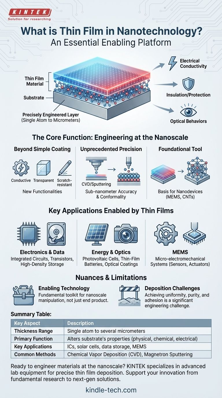
In nanotechnology, a thin film is a precisely engineered layer of material, ranging from a single atom to several micrometers thick, that is applied to a surface or "substrate." This process is not merely a coating; it is a foundational technique used to fundamentally alter the substrate's physical, chemical, or electrical properties. Thin films are the building blocks for many advanced technologies, including integrated circuits, solar cells, and high-density data storage.
Thin film technology is best understood not as an end product, but as an essential enabling platform. It provides the atomic-level control required to build functional nanostructures and engineer the specific material properties needed for cutting-edge devices.
The Core Function: Engineering Properties at the Nanoscale
Thin film technology allows scientists and engineers to construct materials that do not exist in nature by layering different elements with extreme precision.
Beyond Simple Coating
Unlike a conventional layer of paint, a thin film imparts entirely new functionalities to a surface.
These properties can include electrical conductivity, insulation, transparency, scratch resistance, or specific optical behaviors like anti-reflection.
Unprecedented Precision and Control
Deposition techniques, such as Chemical Vapor Deposition (CVD) and magnetron sputtering, can deposit layers with sub-nanometer accuracy.
This means materials can be built up literally one atomic layer at a time, ensuring perfect conformality (uniform coverage over complex shapes) and thickness. This precision is critical when working with nanoparticles or creating quantum-level effects.
A Foundational Tool for Nanomaterials
Thin films are used to coat existing nanomaterials to enhance or protect their properties. They also serve as the basis for fabricating other nanotechnologies.
The ability to create these films is what enables the development of devices like advanced carbon nanotubes and the components within micro-electromechanical systems (MEMS).
Key Applications Enabled by Thin Films
The ability to precisely layer materials is the backbone of modern electronics, energy, and materials science.
Electronics and Data Storage
Every integrated circuit chip is a complex sandwich of thin films. Layers of semiconducting, insulating, and conducting materials are deposited to create the billions of transistors that power our devices. Similarly, high-density hard drives use thin magnetic films to store data.
Energy and Optics
Photovoltaic solar cells are made of multiple thin films, each designed to absorb a different wavelength of light, maximizing energy conversion.
Thin-film batteries offer higher energy densities in smaller packages. Common optical coatings on eyeglasses or camera lenses are thin films designed to reduce glare and reflection.
Micro-electromechanical Systems (MEMS)
MEMS, which include the tiny accelerometers in your phone and airbag sensors in your car, are microscopic machines. They are fabricated by depositing and then selectively etching away successive layers of thin films to create moving parts on a silicon wafer.
Understanding the Nuances and Limitations
While powerful, the role of thin films is often misunderstood. Objectivity requires acknowledging the context in which the technology operates.
Is It "True" Nanotechnology?
A debate exists within the field: does creating a very thin layer alone constitute nanotechnology? Some argue that true nanotechnology involves creating objects with unique nanoscale properties, not just thin versions of bulk materials.
The Enabling Technology Distinction
The most accurate view is that thin film deposition is an enabling technology. The techniques and precision required to create a high-quality thin film are the very same ones needed to fabricate more complex nanostructures.
It provides the fundamental toolkit for manipulating matter at the scale required for "true" nanotechnology, making the distinction largely academic in a practical sense.
Deposition Challenges
Creating a perfect thin film is not trivial. Achieving uniform thickness, purity, and strong adhesion to the substrate over large areas can be a significant engineering and manufacturing challenge. The equipment is sophisticated and can be very expensive, representing a key barrier to entry.
Making the Right Choice for Your Goal
The application of thin film technology depends entirely on your end objective.
- If your primary focus is next-generation electronics: You will leverage thin film deposition to create complex, multi-layered architectures for integrated circuits and high-density memory devices.
- If your primary focus is advanced materials or energy: You will use thin films to create functional surfaces, such as those for photovoltaic cells, efficient batteries, or durable optical coatings.
- If your primary focus is fundamental research: You should view thin film techniques as the essential toolkit for fabricating and manipulating structures at the atomic and molecular level.
Ultimately, mastering thin film deposition is fundamental to translating nanoscale science into real-world technological solutions.
Summary Table:
| Key Aspect | Description |
|---|---|
| Thickness Range | Single atom to several micrometers |
| Primary Function | Alters a substrate's physical, chemical, or electrical properties |
| Key Applications | Integrated circuits, solar cells, data storage, MEMS |
| Common Deposition Methods | Chemical Vapor Deposition (CVD), Magnetron Sputtering |
Ready to engineer materials at the nanoscale? KINTEK specializes in providing the advanced lab equipment and consumables needed for precise thin film deposition. Whether you're developing next-generation electronics, advanced energy solutions, or conducting fundamental research, our expertise supports your innovation. Contact our experts today to discuss how we can enhance your laboratory's capabilities.
Visual Guide
Related Products
- Aluminized Ceramic Evaporation Boat for Thin Film Deposition
- Tungsten Evaporation Boat for Thin Film Deposition
- Electron Beam Evaporation Coating Oxygen-Free Copper Crucible and Evaporation Boat
- Molybdenum Tungsten Tantalum Evaporation Boat for High Temperature Applications
- Aluminum-Plastic Flexible Packaging Film for Lithium Battery Packaging
People Also Ask
- What are thin films deposited by evaporation? A Guide to High-Purity Coating
- What are the applications of thin films deposition? Unlock New Possibilities for Your Materials
- What is thin film deposition? Unlock Advanced Surface Engineering for Your Materials
- What is the chemical method for thin film deposition? Build Films from the Molecular Level Up
- What is the widely used boat made of in thermal evaporation? Choosing the Right Material for High-Purity Deposition


