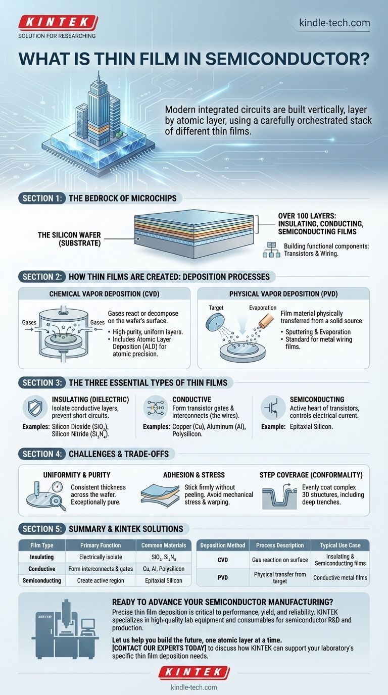
In semiconductor manufacturing, a thin film is a layer of material, ranging from a few micrometers to less than a single nanometer in thickness, that is intentionally deposited onto a silicon wafer. These films are not part of the original silicon crystal but are added in a precise sequence to build the functional components of a microchip, such as transistors and wiring.
The core concept to grasp is that modern integrated circuits are not carved out of a block of silicon. Instead, they are constructed vertically, layer by atomic layer, using a carefully orchestrated stack of different thin films that function as conductors, insulators, and active semiconductor regions.
Why Thin Films are the Bedrock of Microchips
Think of building a microchip like constructing a multi-story skyscraper on a silicon foundation. The thin films are the essential building materials for every part of this structure.
Each layer deposited onto the wafer has a specific electrical or structural purpose. By depositing and then patterning these films, engineers create the complex, three-dimensional architecture that forms billions of transistors and the intricate network of wires connecting them.
The Foundation: The Silicon Wafer
The entire process starts with a highly pure, crystalline silicon wafer. This wafer acts as the substrate, or the fundamental base layer, upon which all subsequent thin film layers are built.
The Building Blocks: Layers Upon Layers
A finished microprocessor can have over 100 distinct layers of material. This stack is composed of a recurring sequence of insulating, conducting, and semiconducting thin films, each contributing to the final circuit.
How Thin Films are Created: Deposition Processes
The process of applying a thin film to a wafer is known as deposition. There are two primary families of deposition techniques, each suited for creating different types of films.
Chemical Vapor Deposition (CVD)
In CVD, the wafer is placed in a chamber and exposed to one or more volatile gases. These gases react or decompose on the wafer's surface, leaving behind a solid material—the thin film.
This method is highly versatile and is used for creating insulating and semiconducting films because the chemical reaction produces very high-purity, uniform layers. A key variant, Atomic Layer Deposition (ALD), allows for building films one single atomic layer at a time, offering unparalleled precision.
Physical Vapor Deposition (PVD)
In PVD, the film material starts as a solid source (a "target"). This material is then physically transferred onto the wafer without a chemical reaction.
The two main PVD methods are sputtering, where high-energy ions bombard the target to knock atoms loose, and evaporation, where the target is heated until it vaporizes. PVD is the standard method for depositing metal films that serve as the circuit's wiring.
The Three Essential Types of Thin Films
Functionally, every film in a semiconductor device falls into one of three categories.
Insulating (Dielectric) Films
These films do not conduct electricity. Their primary job is to isolate conductive layers from one another, preventing short circuits. Silicon Dioxide (SiO₂) and Silicon Nitride (Si₃N₄) are the most common examples.
Conductive Films
These films are the "wires" of the chip, forming the gates of transistors and the interconnects that carry signals between them. Materials include metals like Copper (Cu), Tungsten (W), and Aluminum (Al), as well as heavily doped Polysilicon.
Semiconducting Films
These films are the active heart of the transistors, where the electrical current is actually controlled. The most critical example is epitaxial silicon, a layer of single-crystal silicon grown on the wafer that has pristine quality and precisely controlled electrical properties.
Understanding the Trade-offs and Challenges
Depositing a perfect thin film is an immense technical challenge. The quality of these layers directly impacts the final chip's performance, power consumption, and reliability.
Uniformity and Purity
The film must have a consistent thickness across the entire 300mm wafer. Even a slight variation can cause transistors in one area of the chip to behave differently than those in another. The film must also be exceptionally pure, as a single rogue atom can ruin a device.
Adhesion and Stress
The deposited film must stick firmly to the layer beneath it without peeling or delaminating. Furthermore, the deposition process can create mechanical stress, which can physically warp the wafer or damage the delicate structures built upon it.
Step Coverage (Conformality)
As chips have become more three-dimensional, films must be able to evenly coat the sides and bottoms of deep, narrow trenches. A film that is thick on top but thin on the sides has poor "step coverage" and can create a point of failure.
Connecting Films to Your Goal
The importance of a specific thin film technology depends entirely on the engineering objective.
- If your primary focus is transistor performance: The quality of the ultra-thin gate dielectric and the purity of the epitaxial silicon semiconductor film are paramount.
- If your primary focus is chip speed: The key is mastering the deposition of low-resistance conductive films (like copper) for interconnects and low-k dielectric films to insulate them.
- If your primary focus is manufacturing yield: The goal is perfecting deposition processes to ensure absolute film uniformity, purity, and conformality across every wafer.
Ultimately, mastering the science of creating and controlling thin films is the fundamental requirement for advancing modern electronics.
Summary Table:
| Film Type | Primary Function | Common Materials |
|---|---|---|
| Insulating (Dielectric) | Electrically isolate conductive layers | Silicon Dioxide (SiO₂), Silicon Nitride (Si₃N₄) |
| Conductive | Form transistor gates and interconnects (wires) | Copper (Cu), Aluminum (Al), Polysilicon |
| Semiconducting | Create the active region of transistors | Epitaxial Silicon |
| Deposition Method | Process Description | Typical Use Case |
| Chemical Vapor Deposition (CVD) | Gases react on wafer surface to form a solid film | High-purity insulating & semiconducting films |
| Physical Vapor Deposition (PVD) | Solid target material is physically transferred to wafer | Conductive metal films for wiring |
Ready to Advance Your Semiconductor Manufacturing?
The precise deposition of thin films is critical to your chip's performance, yield, and reliability. KINTEK specializes in providing high-quality lab equipment and consumables for semiconductor R&D and production. Whether your focus is on achieving perfect uniformity with CVD systems or depositing low-resistance metals via PVD, our solutions are designed to meet the stringent demands of modern semiconductor fabrication.
Let us help you build the future, one atomic layer at a time. Contact our experts today to discuss how KINTEK can support your laboratory's specific thin film deposition needs.
Visual Guide