In short, a vast range of materials can be used in thin film deposition, including pure metals, alloys, ceramics, semiconductors, and even organic compounds. The specific material is always chosen based on the desired physical, electrical, or optical properties of the final film, such as conductivity, hardness, or transparency.
The central takeaway is that the material is not an isolated choice. It is part of a system where the material, the deposition method (e.g., sputtering vs. evaporation), and the final application are all deeply interconnected.

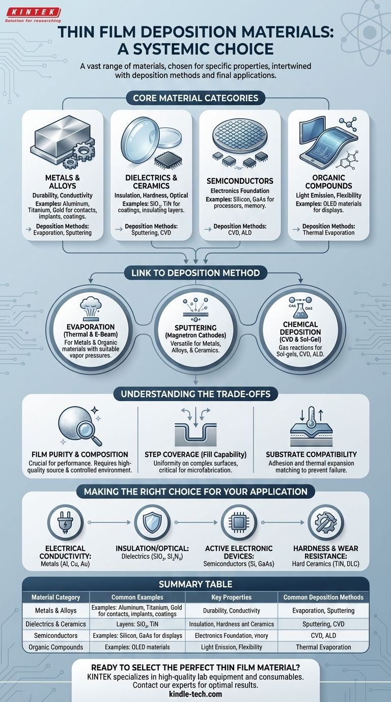
Core Material Categories in Thin Film Deposition
The materials used for creating thin films are selected to impart specific characteristics onto a substrate's surface. They generally fall into a few key categories.
Metals and Alloys
Metals are frequently used due to their durability, excellent thermal and electrical conductivity, and relative ease of deposition.
Common examples include aluminum for reflective coatings and electrical contacts, titanium for biocompatible medical implants, and gold for corrosion-resistant contacts.
Dielectrics and Ceramics
These materials are used for their insulating properties, hardness, or specific optical characteristics. They are essential for creating anti-reflective coatings on lenses or insulating layers in microchips.
Materials like silicon dioxide (SiO₂) and titanium nitride (TiN) are common examples, often deposited using sputtering or chemical vapor deposition methods.
Semiconductors
Semiconductor materials are the foundation of the entire electronics industry. Thin film deposition is the core process used to build up the complex layered structures in processors and memory chips.
Polycrystalline silicon, silicon-based epitaxial films, and various compound semiconductors like gallium arsenide (GaAs) are staples in this category.
Organic Compounds
Certain deposition techniques, particularly thermal evaporation, are well-suited for depositing thin layers of organic materials.
These films are critical for applications like manufacturing OLED (Organic Light-Emitting Diode) displays for phones and televisions.
How Material Choice is Linked to Deposition Method
The properties of a material dictate which deposition method will be most effective. A source material that melts easily cannot be used in a high-temperature chemical process.
Evaporation (Thermal & E-Beam)
Evaporation sources are ideal for materials that can be heated in a vacuum until they turn into a vapor, which then condenses on the substrate.
This method works well for many metals and organic materials with suitable vapor pressures.
Sputtering (Magnetron Cathodes)
Sputtering is a physical process where ions bombard a target material, knocking atoms loose that then deposit onto the substrate.
This is a highly versatile technique suitable for a very broad range of materials, including metals, alloys, and ceramics that are difficult or impossible to evaporate.
Chemical Deposition (CVD & Sol-Gel)
In chemical processes, the film is formed from precursor gases or solutions that react on the substrate surface.
Sol-gels, for instance, are liquid solutions containing nanoparticles that form an even ceramic or oxide layer as the liquid is removed. This approach is a key part of chemical vapor deposition (CVD) and atomic layer deposition (ALD).
Understanding the Key Trade-offs
Selecting a material involves more than just its primary function. You must consider several practical constraints that determine success or failure.
Film Purity and Composition
Unintentional impurities or slight variations in composition can dramatically alter the performance of the final film.
Achieving the desired film requires high-quality source materials and precise control over the deposition chamber's environment to prevent contamination.
Step Coverage (Fill Capability)
Step coverage describes how uniformly a film coats a substrate with a complex, non-flat surface, such as the trenches in a microchip.
Some deposition methods provide excellent, uniform coverage over any shape, while others create thicker layers on top surfaces and thinner layers on sidewalls, a critical trade-off in microfabrication.
Substrate Compatibility
The chosen material must adhere well to the substrate. Poor adhesion can cause the film to peel, crack, or delaminate, rendering the component useless. The material's thermal expansion properties must also be compatible with the substrate to prevent stress during heating or cooling.
Making the Right Choice for Your Application
Your end goal dictates the ideal material. The function of the final product is the most important factor in the selection process.
- If your primary focus is electrical conductivity: Metals like aluminum, copper, or gold are the standard choices for wiring and contact metallization.
- If your primary focus is insulation or optical coatings: Dielectric materials like silicon dioxide (SiO₂), silicon nitride (Si₃N₄), or aluminum oxide (Al₂O₃) are ideal.
- If your primary focus is creating active electronic devices: Semiconductor materials like silicon (Si) or compound semiconductors are non-negotiable.
- If your primary focus is hardness and wear resistance: Hard ceramics like titanium nitride (TiN) or diamond-like carbon (DLC) are used for protective coatings on tools and implants.
Ultimately, material selection is the strategic first step that defines the capabilities and limitations of your final product.
Summary Table:
| Material Category | Common Examples | Key Properties | Common Deposition Methods |
|---|---|---|---|
| Metals & Alloys | Aluminum, Gold, Titanium | High conductivity, durability, reflectivity | Evaporation, Sputtering |
| Dielectrics & Ceramics | Silicon Dioxide (SiO₂), Titanium Nitride (TiN) | Insulation, hardness, optical coatings | Sputtering, CVD |
| Semiconductors | Silicon, Gallium Arsenide (GaAs) | Active electronic properties | CVD, ALD |
| Organic Compounds | OLED materials | Light emission, flexibility | Thermal Evaporation |
Ready to Select the Perfect Thin Film Material for Your Project?
Choosing the right material and deposition method is critical to your product's performance. KINTEK specializes in providing high-quality lab equipment and consumables for all your thin film deposition needs, from research to production.
We understand the intricate balance between material properties, deposition techniques, and your application's requirements. Our experts can help you navigate these choices to achieve optimal results in conductivity, hardness, or optical performance.
Let's discuss your specific application challenges and goals. Contact our team today to find the ideal solution for your laboratory.
Visual Guide
Related Products
- Aluminized Ceramic Evaporation Boat for Thin Film Deposition
- Tungsten Evaporation Boat for Thin Film Deposition
- Molybdenum Tungsten Tantalum Evaporation Boat for High Temperature Applications
- Electron Beam Evaporation Coating Oxygen-Free Copper Crucible and Evaporation Boat
- Hemispherical Bottom Tungsten Molybdenum Evaporation Boat
People Also Ask
- Why is an alumina boat selected for catalyst precursors? Ensure Sample Purity at 1000 °C
- What is thin film deposition? Unlock Advanced Surface Engineering for Your Materials
- What are the applications of thin films deposition? Unlock New Possibilities for Your Materials
- Why are high-purity ceramic boats used for lignin activation? Ensure Purity & Thermal Stability
- What are thin films deposited by evaporation? A Guide to High-Purity Coating


