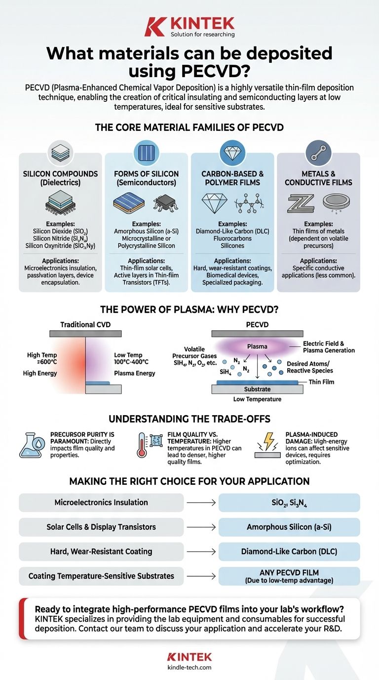
In short, PECVD can deposit a wide range of materials, including dielectric insulators, semiconductors, and specialized polymers. The most common materials are silicon-based compounds such as silicon dioxide (SiO₂), silicon nitride (Si₃N₄), and amorphous silicon (a-Si), which are fundamental to the microelectronics industry.
Plasma-Enhanced Chemical Vapor Deposition (PECVD) is a highly versatile thin-film deposition technique. Its primary advantage is using a plasma to drive chemical reactions at low temperatures, making it ideal for depositing critical insulating and semiconducting layers onto substrates that cannot withstand the heat of traditional methods.
The Core Material Families of PECVD
PECVD's versatility stems from its ability to handle different precursor gases, allowing for the creation of diverse thin films. These materials generally fall into a few key categories based on their composition and application.
Silicon Compounds (Dielectrics)
The most prevalent use of PECVD is for depositing high-quality dielectric films. These materials are electrical insulators crucial for manufacturing integrated circuits.
The key materials include **silicon dioxide (SiO₂) **, silicon nitride (Si₃N₄), and silicon oxynitride (SiOxNy). They serve as insulating layers between conductive paths, as protective passivation layers, and as device encapsulation to shield components from moisture and contamination.
Forms of Silicon (Semiconductors)
PECVD is also used to deposit forms of silicon itself, which act as semiconductors.
This includes amorphous silicon (a-Si) and microcrystalline or polycrystalline silicon. These films are essential for applications like thin-film solar cells and the active layers in thin-film transistors (TFTs) used in flat-panel displays.
Carbon-Based and Polymer Films
Beyond silicon, PECVD can create specialized carbon-based coatings and polymers.
Diamond-Like Carbon (DLC) is a prominent example, valued for its extreme hardness and low friction. It is frequently used as a protective coating in tribological applications to reduce wear on mechanical parts.
The process can also deposit organic and inorganic polymers, such as fluorocarbons and silicones, for specialized uses in biomedical devices and advanced food packaging.
Metals and Conductive Films
While less common than for dielectrics, PECVD can be used to deposit thin films of metals. The specific metal depends on the availability of a suitable volatile precursor gas.
Why PECVD is the Chosen Method
Understanding the process itself reveals why it's so well-suited for these materials. The choice of PECVD is often driven by its unique operational advantage: low temperature.
The Power of Plasma
In traditional Chemical Vapor Deposition (CVD), high temperatures (often >600°C) are required to provide the energy needed for precursor gases to react and form a film.
In PECVD, an electric field generates a plasma, which energizes the gas molecules. This plasma provides the necessary reaction energy, allowing the deposition to occur at much lower temperatures, typically between 100°C and 400°C.
The Requirement for Volatile Precursors
The entire process hinges on the use of volatile precursor gases. These are chemical compounds that contain the atoms desired for the film (e.g., silane gas, SiH₄, for silicon films) and can be easily transported in a vapor state. The plasma breaks these precursors down, and the desired atoms deposit onto the substrate surface.
Understanding the Trade-offs
While powerful, PECVD is not without its limitations and required considerations. Achieving a high-quality film requires careful control over the process variables.
Precursor Purity is Paramount
The quality of the final film is directly tied to the purity of the precursor gases. Any impurities in the gas source risk being incorporated into the deposited film, which can degrade its electrical or mechanical properties.
Film Quality vs. Temperature
There is often a trade-off between deposition temperature and film quality. Even within PECVD's low-temperature window, films deposited at slightly higher temperatures tend to be denser and have better structural integrity. The process must be optimized to balance the substrate's heat tolerance with the desired film characteristics.
Potential for Plasma-Induced Damage
The high-energy ions within the plasma can sometimes cause physical or electrical damage to the substrate or the growing film. This is a critical consideration when depositing on sensitive electronic devices, and process parameters must be tuned to minimize this effect.
Making the Right Choice for Your Application
Selecting a material and process depends entirely on your end goal. PECVD offers a solution for a wide range of modern engineering challenges.
- If your primary focus is microelectronics insulation: Your ideal materials are high-purity silicon dioxide (SiO₂) and silicon nitride (Si₃N₄) for their excellent dielectric and passivation properties.
- If your primary focus is solar cells or display transistors: Amorphous silicon (a-Si) is the standard choice for the active semiconductor layer in these devices.
- If your primary focus is a hard, wear-resistant coating: Diamond-Like Carbon (DLC) is the industry-leading material for tribological performance.
- If your primary focus is coating a temperature-sensitive substrate: PECVD's fundamental low-temperature advantage makes it the superior method for depositing any of these films onto polymers, plastics, or fully fabricated devices.
Ultimately, PECVD's ability to create high-performance films without high heat makes it an indispensable tool in modern materials engineering.
Summary Table:
| Material Category | Key Examples | Primary Applications |
|---|---|---|
| Silicon Compounds (Dielectrics) | Silicon Dioxide (SiO₂), Silicon Nitride (Si₃N₄) | Microelectronics insulation, passivation layers |
| Silicon (Semiconductors) | Amorphous Silicon (a-Si) | Thin-film solar cells, display transistors (TFTs) |
| Carbon-Based Films | Diamond-Like Carbon (DLC) | Hard, wear-resistant protective coatings |
| Polymer Films | Fluorocarbons, Silicones | Biomedical devices, specialized packaging |
Ready to integrate high-performance PECVD films into your lab's workflow? KINTEK specializes in providing the lab equipment and consumables you need to successfully deposit these critical materials. Our expertise ensures you achieve optimal film quality and process efficiency. Contact our team today to discuss how we can support your specific application and accelerate your research and development.
Visual Guide
Related Products
- Inclined Rotary Plasma Enhanced Chemical Vapor Deposition PECVD Equipment Tube Furnace Machine
- Chemical Vapor Deposition CVD Equipment System Chamber Slide PECVD Tube Furnace with Liquid Gasifier PECVD Machine
- Inclined Rotary Plasma Enhanced Chemical Vapor Deposition PECVD Equipment Tube Furnace Machine
- RF PECVD System Radio Frequency Plasma-Enhanced Chemical Vapor Deposition RF PECVD
- Multi Heating Zones CVD Tube Furnace Machine Chemical Vapor Deposition Chamber System Equipment
People Also Ask
- What is the necessity of depositing a silicon nitride (SiNx) thin film using PECVD? Optimize QSSPC Lifetime Measurement
- What is plasma enhanced chemical vapor deposition PECVD equipment? A Guide to Low-Temperature Thin Film Deposition
- Why is a PECVD system required for vertical graphene synthesis? Master Directional Control for 3D Nanostructures
- What is plasma enhanced chemical vapour deposition PECVD used for? Enable Low-Temp Thin Films for Electronics & Solar
- What are the core advantages of PE-CVD in OLED encapsulation? Protect Sensitive Layers with Low-Temp Film Deposition


