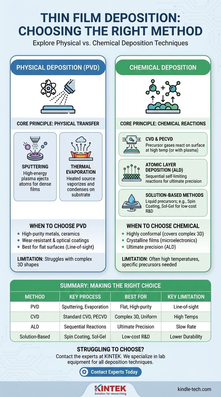
The definitive answer is that there is no single method for thin film deposition. Instead, techniques are broadly divided into two fundamental categories: Physical Deposition and Chemical Deposition. Physical methods physically transfer a material from a source to a substrate, while chemical methods use chemical reactions on the substrate's surface to grow the film.
The choice between a physical or chemical method is not arbitrary. It is a critical engineering decision determined by the specific material being deposited, the required film properties like thickness and uniformity, and the geometry of the part being coated.
Understanding Physical Vapor Deposition (PVD)
Physical Vapor Deposition (PVD) refers to a family of processes where a material is converted into a vapor phase in a vacuum, transported across the chamber, and condensed onto a substrate to form a thin film.
The Core Principle: Physical Transfer
Think of PVD as a highly controlled, atom-by-atom spray-painting process occurring in a vacuum. No fundamental chemical reactions are intended to happen.
The process involves generating vapor from a solid source material (known as the target) and having it deposit onto the item you wish to coat (the substrate).
Common Method: Sputtering
Sputtering is one of the most versatile PVD techniques. It uses a high-energy plasma, typically from an inert gas like Argon, to bombard the target material.
This bombardment ejects or "sputters" atoms from the target, which then travel and deposit onto the substrate, forming a dense and uniform film.
Common Method: Thermal Evaporation
Thermal evaporation is conceptually simpler. The source material is heated in a vacuum until it evaporates or sublimes into a gaseous form.
This gas then travels through the vacuum chamber and condenses on the cooler substrate, much like water vapor condenses on a cold glass.
Exploring Chemical Deposition Methods
Chemical deposition methods use chemical precursors—often in a gaseous or liquid state—that react on or near the substrate surface to form the desired film.
The Core Principle: Building Films from Chemical Reactions
Unlike PVD, these methods build the film through controlled chemical change. The composition of the final film can be different from the precursor materials.
Common Method: Chemical Vapor Deposition (CVD)
In a CVD process, the substrate is exposed to one or more volatile precursor gases. These gases react or decompose on the substrate's surface at high temperatures, leaving behind a solid film.
A variation, Plasma-Enhanced CVD (PECVD), uses a plasma to energize the gases, allowing the process to run at much lower temperatures.
Precision Method: Atomic Layer Deposition (ALD)
Atomic Layer Deposition (ALD) is a subtype of CVD that offers the highest level of precision. It uses a sequence of self-limiting chemical reactions to deposit material one single atomic layer at a time.
This provides exceptional control over film thickness and the ability to coat extremely complex, high-aspect-ratio structures with perfect uniformity.
Solution-Based Methods: Sol-Gel and Spin Coating
Techniques like sol-gel, spin coating, and dip coating are chemical methods that begin with a liquid precursor. The substrate is coated with the liquid, and the film is formed as the liquid is dried, cured, or heated.
These methods are often lower-cost and well-suited for applications like polymer films, optical coatings, and lab-scale research.
Understanding the Trade-offs
Choosing the right method requires understanding the inherent advantages and limitations of each category.
When to Choose PVD
PVD is often favored for its ability to deposit a very wide range of materials, including metals, alloys, and ceramics, with high purity and density.
It is the dominant method for applications requiring wear-resistant coatings on tools, metallization in semiconductor manufacturing, and reflective optical coatings.
When to Choose CVD
CVD excels at producing highly conformal coatings, meaning it can uniformly cover complex, non-flat surfaces. This is a significant advantage over PVD, which is largely a line-of-sight process.
CVD is also ideal for creating very high-purity, high-performance crystalline films, such as the silicon layers essential for microelectronics.
Key Limitations to Consider
PVD struggles to uniformly coat complex 3D shapes. CVD processes often require very high temperatures, which can damage sensitive substrates, and depend on the availability of suitable volatile precursor chemicals.
Making the Right Choice for Your Application
Your specific goal dictates the best deposition strategy.
- If your primary focus is a high-purity metallic or hard ceramic coating on a relatively flat surface: Sputtering (PVD) is the most robust and common choice.
- If your primary focus is a perfectly uniform coating on a complex 3D object: Chemical Vapor Deposition (CVD) is the superior technology.
- If your primary focus is ultimate precision and creating films just a few atoms thick: Atomic Layer Deposition (ALD) is the only viable option.
- If your primary focus is low-cost lab-scale development or depositing organic materials: Solution-based methods like Spin Coating or Sol-Gel are excellent starting points.
Selecting the right deposition technique is the foundational step in engineering a film with the precise properties your application demands.
Summary Table:
| Method Category | Key Process | Best For | Key Limitation |
|---|---|---|---|
| Physical Vapor Deposition (PVD) | Sputtering, Thermal Evaporation | High-purity metals/ceramics, flat surfaces | Line-of-sight, struggles with complex 3D shapes |
| Chemical Vapor Deposition (CVD) | Standard CVD, PECVD | Uniform coatings on complex 3D objects | High temperatures, specific precursors needed |
| Atomic Layer Deposition (ALD) | Sequential self-limiting reactions | Ultimate precision, atomic-level thickness | Slower deposition rate |
| Solution-Based Methods | Spin Coating, Sol-Gel | Low-cost R&D, organic materials | Film quality and durability may be lower |
Struggling to choose the right thin film deposition method for your project? The experts at KINTEK are here to help. We specialize in lab equipment and consumables for all deposition techniques, from robust PVD sputtering systems to precise ALD reactors. We can guide you to the ideal solution for your material, substrate, and performance requirements.
Contact our experts today to discuss your specific application and discover how KINTEK can enhance your laboratory's capabilities and ensure your project's success.
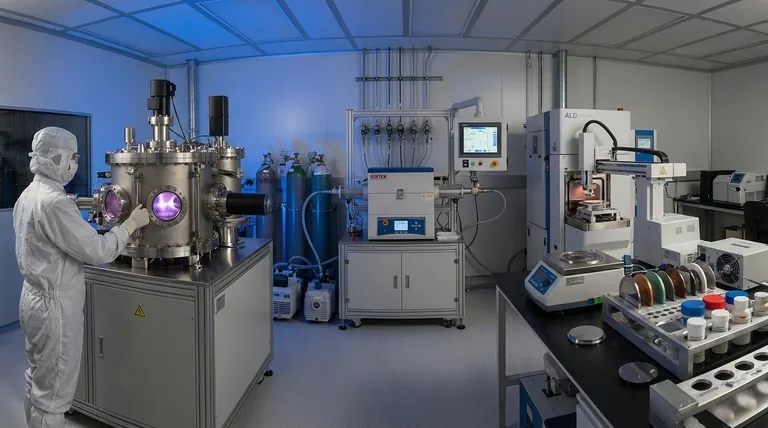
Visual Guide
Related Products
- Aluminized Ceramic Evaporation Boat for Thin Film Deposition
- Tungsten Evaporation Boat for Thin Film Deposition
- Electron Beam Evaporation Coating Oxygen-Free Copper Crucible and Evaporation Boat
- Molybdenum Tungsten Tantalum Evaporation Boat for High Temperature Applications
- Vacuum Hot Press Furnace Machine for Lamination and Heating
People Also Ask
- Why are high-purity ceramic boats used for lignin activation? Ensure Purity & Thermal Stability
- What are the alternatives to sputtering? Choose the Right Thin Film Deposition Method
- Why is an alumina boat and Ti3AlC2 powder bed necessary for Ti2AlC sintering? Protect MAX Phase Purity
- What is the widely used boat made of in thermal evaporation? Choosing the Right Material for High-Purity Deposition
- What is the chemical method for thin film deposition? Build Films from the Molecular Level Up


