In short, Physical Vapor Deposition (PVD) is used across a vast range of industries to apply high-performance thin films onto surfaces. Key sectors include aerospace for temperature-resistant components, electronics for creating optical films on semiconductors and solar panels, and manufacturing for applying hard, corrosion-resistant coatings to cutting tools.
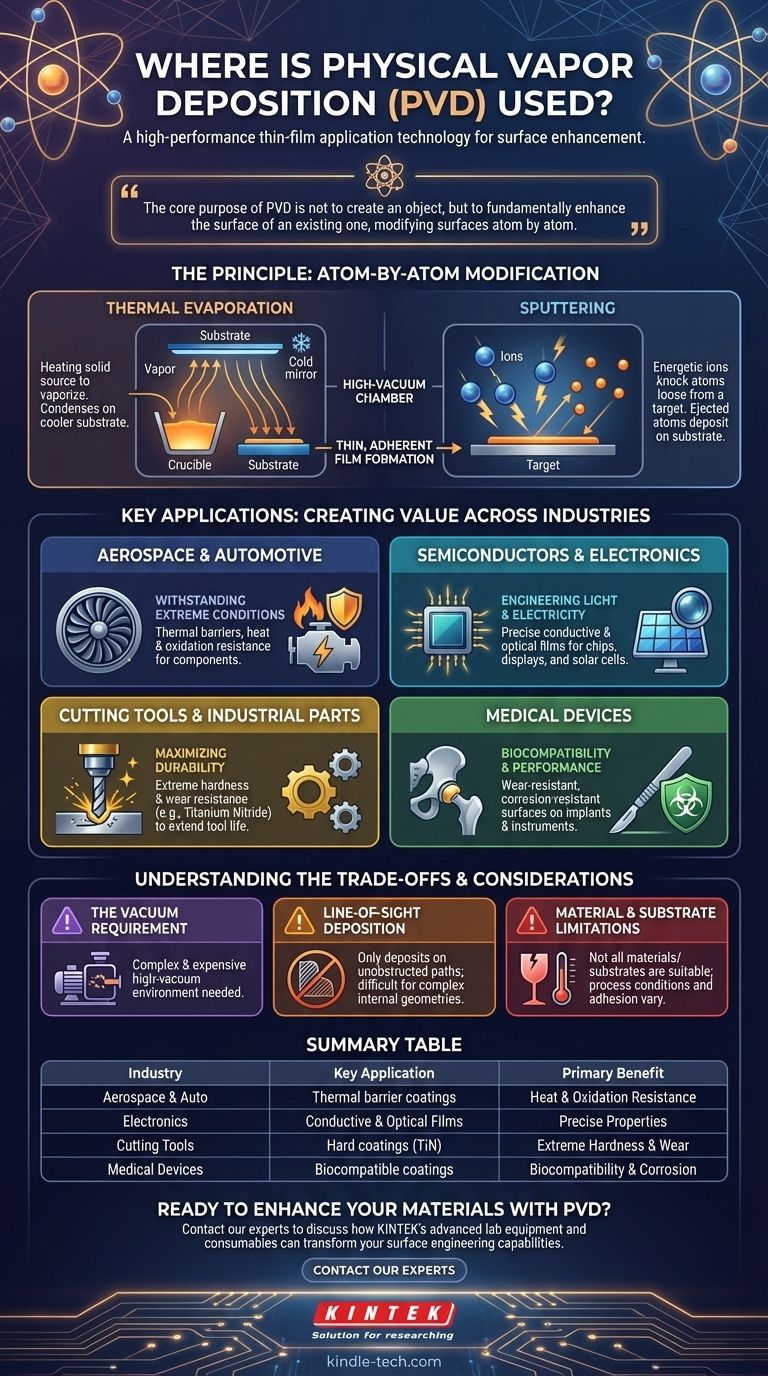
The core purpose of PVD is not to create an object, but to fundamentally enhance the surface of an existing one. It is a powerful surface engineering tool used to grant materials new properties—like extreme hardness, biocompatibility, or specific optical characteristics—that they do not inherently possess.
The Principle of PVD: Modifying Surfaces Atom by Atom
What is Physical Vapor Deposition?
Physical Vapor Deposition is a family of vacuum deposition methods. In a high-vacuum chamber, a solid source material is converted into a vapor through a physical process, such as heating or bombardment with ions.
This vapor then travels across the chamber and condenses on the target object—the substrate—forming a thin, highly adherent film. The process is essentially moving a material from a source to a substrate, one atom or molecule at a time.
Key Techniques: Evaporation vs. Sputtering
The two most common PVD techniques are thermal evaporation and sputtering.
Thermal evaporation involves heating a material until it vaporizes. This vapor then deposits onto the cooler substrate, much like steam condensing on a cold mirror.
Sputtering is a more energetic process. Here, a solid "target" of the coating material is bombarded with high-energy ions, which physically knock atoms loose. These ejected atoms then deposit onto the substrate.
Where PVD Creates Value: Key Applications
Aerospace and Automotive: Withstanding Extreme Conditions
Components in aerospace and high-performance automotive engines face extreme temperatures and stresses. PVD is used to apply dense, temperature-resistant ceramic coatings.
These films act as thermal barriers, protecting the underlying metal from heat damage and oxidation, thereby extending the component's lifespan and reliability.
Semiconductors and Electronics: Engineering Light and Electricity
The microelectronics industry relies on depositing extremely thin and pure films with precise properties. PVD is critical for this.
It is used to create the conductive layers in microchips, apply anti-reflective optical films for solar panels and lenses, and even produce holographic displays. The high degree of control PVD offers is essential for these nanoscale applications.
Cutting Tools and Industrial Parts: Maximizing Durability
One of the most common uses for PVD is applying hard coatings to industrial tools, such as drill bits and milling cutters.
Films like Titanium Nitride (TiN) are exceptionally hard and reduce friction. This allows tools to cut faster, last significantly longer, and resist wear and corrosion, even in the harshest manufacturing environments.
Medical Devices: Biocompatibility and Performance
In the medical field, PVD coatings are used on surgical instruments and implants. These films provide a hard, wear-resistant surface that can also be engineered to be biocompatible.
This means the coating prevents adverse reactions with the human body, reduces the risk of corrosion, and can even provide color-coding for surgical instruments.
Understanding the Trade-offs of PVD
The Vacuum Requirement
PVD processes must be conducted in a high-vacuum environment. This is necessary to prevent the vaporized coating atoms from colliding with air molecules.
This requirement means PVD equipment is complex and expensive, representing a significant capital investment.
Line-of-Sight Deposition
Most PVD processes are "line-of-sight," meaning the coating can only deposit on surfaces that have a direct, unobstructed path from the source material.
Coating the inside of complex shapes or shadowed areas is extremely difficult. This is a primary limitation compared to other methods like Chemical Vapor Deposition (CVD), which can coat more uniformly.
Material and Substrate Limitations
While versatile, not all materials can be effectively deposited via PVD, and not all substrates can withstand the process conditions, which can involve elevated temperatures.
The adhesion and quality of the film are highly dependent on the choice of materials, substrate preparation, and process parameters, requiring a high degree of technical expertise to execute correctly.
Making the Right Choice for Your Goal
PVD is a specialized process chosen for the unique surface properties it delivers. To determine if it's right for you, consider the primary property you need to enhance.
- If your primary focus is extreme hardness and wear resistance: PVD is a leading choice for applying ceramic films to tools, molds, and high-wear mechanical components.
- If your primary focus is precise optical or electronic properties: The control offered by PVD makes it ideal for building the thin, multi-layered films required in semiconductors, optics, and solar cells.
- If your primary focus is biocompatibility or a decorative finish: PVD is widely used to create inert, durable, and colorful coatings for medical implants, watches, and hardware.
- If you must coat complex, internal geometries: Standard PVD may not be suitable, and you should investigate alternative methods or more specialized PVD techniques.
Ultimately, Physical Vapor Deposition is a transformative technology that allows us to engineer the surface of a material to achieve performance far beyond its natural limits.
Summary Table:
| Industry | Key Application | Primary Benefit |
|---|---|---|
| Aerospace & Automotive | Thermal barrier coatings on engine components | Heat & oxidation resistance |
| Semiconductors & Electronics | Conductive & optical films for chips & solar panels | Precise electrical/optical properties |
| Cutting Tools & Industrial Parts | Hard coatings (e.g., Titanium Nitride) on drill bits | Extreme hardness & wear resistance |
| Medical Devices | Biocompatible coatings on implants & instruments | Biocompatibility & corrosion resistance |
Ready to enhance your materials with high-performance PVD coatings?
KINTEK specializes in advanced lab equipment and consumables for precise Physical Vapor Deposition processes. Whether you're developing cutting tools, semiconductor components, or medical implants, our solutions deliver the extreme hardness, precise optical properties, and biocompatibility your projects demand.
Contact our experts today to discuss how KINTEK's PVD technology can transform your surface engineering capabilities and bring your most challenging material designs to life.
Visual Guide
Related Products
- Electron Beam Evaporation Coating Oxygen-Free Copper Crucible and Evaporation Boat
- Custom CVD Diamond Coating for Lab Applications
- Molybdenum Tungsten Tantalum Special Shape Evaporation Boat
- HFCVD Machine System Equipment for Drawing Die Nano-Diamond Coating
- Infrared Transmission Coating Sapphire Sheet Substrate Window
People Also Ask
- How is an electron beam evaporator cooled during deposition? Essential Thermal Management for Stable Processes
- What is the voltage of e-beam evaporation? Achieve Precise Thin-Film Deposition
- What is the current of e-beam evaporation? A Guide to High-Purity Thin Film Deposition
- What is e-beam evaporation used for? Precision Coating for Optics, Aerospace & Electronics
- What is the deposition rate of e-beam evaporation? Control Thin Film Quality and Speed


